Although it’s over 10 years old now the Xilinx now AMD Zynq-7000 System-on-Chip is still pretty popular both among hobbyists and professional embedded developers. Yet, there is not much information about the raw performance of the SoC available out there. To help remedy that, and also give us a baseline to compare with when we publish a follow-up article on the performance of the Zynq Ultrascale+ MPSoC, we’ve decided to write this article.
In this article, we’ll follow the methodology we used in a previous couple of articles that ended up being quite popular where we looked at some bare-metal benchmarks of the Xilinx MicroBlaze. (See part 1 and part 2). We’ll start with well-known synthetic CPU benchmarks, namely CoreMARK, Dhrystone, Whetstone and Linpack. Following that, we’ll look at the memory bandwidth and latency of the external DDR memory, On-Chip RAM and block RAM (BRAM) instantiated in the FPGA. Finally, we’ll round up the article with some numbers on interrupt latency.
The Zynq-7000
Before diving into the benchmarks, let’s take the time to look at the architecture of the Zynq-7000. To help with the discussion, Figure 1 below shows a simplified block diagram of the SoC based on Figure 5-1 from the Zynq-7000 Technical Reference Manual.
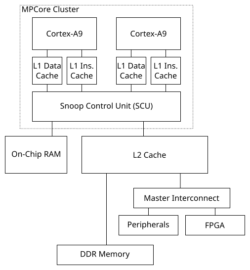
The Zynq-7000 is comprised of two ARM Cortex-A9 dual-pipeline CPU cores with out-of-order execution arranged in an MPCore multiprocessing cluster. Each ARM core has a separate L1 data and instruction caches of 32 KiB each. Both cores are connected to a Snoop Control Unit (SCU) which maintains coherency between the data cache of both cores. The CPU cluster is connected to a 512 KiB unified L2 cache. The CPU cluster also has a privileged data path directly from the SCU to 256 KiB of On-Chip RAM (OCRAM). The OCRAM and L2 cache are clocked at the same rate and have similar low access latency. The L2 cache master port has a direct connection to the external DDR memory controller, minimizing the access latency of the main memory.
From the CPU point of view, the peripherals, including the FPGA through the General Purpose AXI slave port, are accessed from the master interconnect. Although not shown in the diagram, the FPGA can also access the peripherals through the central interconnect using the AXI General Purpose master ports. The FPGA can also access the external DDR memory and the OCRAM through the central interconnect. Finally, the FPGA has a direct data path to the external DDR memory and OCRAM through the AXI High Performance master ports.
Which Speed Grade
Although most of the Zynq-7000 marketing material mentions a maximum CPU core clock speed of 1 GHz, this is only possible for a XC7Z030 or XC7Z045 device of speed grade -3 which are out of reach for most applications. XC7Z020 and XC7Z010 devices can have a maximum clock speed of 866 MHz again for the -3 speed grade. The single core 7000S devices are further limited to a 766 MHz. Every device in the Zynq-7000 family can reach 666 MHz when selecting a more common speed grade of -1.
A similar situation arises with the DDR bus frequency, XC7Z030 or XC7Z045 devices of speed grade -3 can reach a DDR speed of 1333 MT/s using DDR3 memory. That being said, most other devices and speed grades can reach 1066 MT/s, even speed grade -1 devices.
So in order for the following benchmarks to be representative of a typical high performance applications, we’ve selected a clock speed of 800 MHz with a DDR bus speed of 1066 MT/s running DDR3 memory which represents a good middle-of-the-road Zynq-7000 of speed grade -2.
Finally, the Zynq-7000 uses a fixed ratio between the clock frequency of the CPU, L2 memory subsystem and the master interconnect. The usual configuration has the L2 subsystem clocked at 1/3 of the CPU core clock frequency and the peripheral APB bus running at half the frequency of the L2 subsystem. This configuration is known as the 6:2:1 configuration. It is also possible to use an alternative 4:2:1 configuration which limits the maximum CPU frequency but allows a slightly higher bus frequency. The 4:2:1 is not generally useful except for applications that need to maximize the bus speed or perhaps for some low-power applications. As such, we’ll be using the default 6:2:1 clock configuration.
CPU Benchmarks
Let’s start by looking at the core CPU performances. Running and publishing CPU benchmarks targeting embedded platforms isn’t a simple matter. Especially when applied to bare-metal benchmarks which are more representative for embedded designs running an RTOS or bare-metal. The best benchmark is to measure the performance of the final application which isn’t possible when aiming at a generic benchmark. We could craft a realistic RTOS workload but we strongly believe that benchmark results should be reproducible independently by readers. To this end, we fall back to four well-known benchmarks. Namely the venerated Dhrystone and more recent EEMBC CoreMark for integer performance. For floating point, we’ll go for a double precision Whetstone and a traditional 100×100 Linpack also using double precision.
All of the benchmarks were ported in order to run on a bare-metal target using Xilinx’s distribution of GCC 10.2.0 with optimization set at -O2. The linker was instructed to link the application code and data to the external DDR SDRAM.
There’s a lot of versions and variations available around the internet for most of the benchmarks used in this article. For reference, the Dhrystone implementation we used is Rick Richardson’s C translation of Dhrystone 2.1 downloaded from Roy Longbottom’s Dhrystone result page. The CoreMark implementation is version 1.01 taken from the EEMBC GitHub. The Whetstone version used is the one distributed by Roy Longbottom and finally we use Jack Dongarra’s Linpack C source.
| Benchmark | Result | Per MHz |
|---|---|---|
| Dhrystone (MIPS) | 2096 | 2.62 |
| CoreMark | 2970 | 3.71 |
| Whetstone (MWIPS) | 842 | 1.05 |
| Linpack (MFLOPS) | 143 | 0.18 |
The results show a single core performance of 2.62 Dhrystone MIPS/MHz and 3.71 CoreMark per MHz which are fairly close to published values from ARM and the EEMBC results database. It’s harder to compare floating-point performances since there aren’t many results published for Whetstone and Linpack on embedded platforms and many of those results were published with much older compilers. Roy Longbottom, however, has published quite a comprehensive list of Dhrystone, Whetstone and Linpack results which can be used for comparisons. In all cases, the results in this article are mostly to act as a baseline for a future article on the Zynq UltraScale+ performances.
Memory Access Bandwidth and Latency
In this section, we’ll look at the bandwidth and latency of the various memories available within the Zynq-7000. More precisely, we’ll benchmark the full external DDR memory hierarchy, including the L1 and L2 caches, the on-chip RAM as well as some block RAM (BRAM) located within the FPGA. The methods used here are similar to those previously used in our article looking at the MicroBlaze memory performances. It’s important to note that all of these results are for single-core performances using a synthetic access pattern.
It’s tricky to present performance data on memory bandwidth since it depends so much on the access pattern, especially when multiple masters are involved with a mix of read and writes. Also which operation (read vs write, sequential vs random etc.) is measured will change the result considerably. For example, sustained writes to cacheable or even device memory are usually posted meaning they are acknowledged early and the CPU doesn’t need to wait for the actual write to complete, it only needs to wait for the bus to accept the write. On the other hand, reading requires sending the read request down the bus and waiting for the answer.
External DDR Memory Bandwidth and Latency
The memory read and write bandwidths versus the working set for the external DDR3 are shown in the next figure. Since the DDR memory region is mapped as normal cacheable memory, this is very informative as it shows the bandwidth of accessing the L1 and L2 cache as well as the external memory.
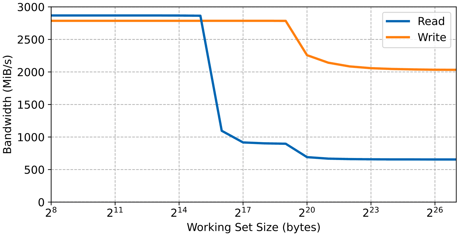
The bandwidth is measured by performing in a loop sequential aligned double-word (8 bytes) accesses over a region of memory. Being sequential, these bandwidths include the effect of the cache prefetching.
The access latency is even trickier to measure than measuring the bandwith. First, as mentioned previously, writes are posted for normal memory which means they seem to happen very quickly from the point of view of the CPU. As such, only the read latency yields interesting results. Second, the Cortex-A9 being an out-of-order pipelined processor with both L1 and L2 automatic prefetchers it’s necessary to carefully craft the memory access pattern to prevent those features from affecting the result. For this article the benchmark is performed in a similar fashion to the well-known LMBENCH by dividing the memory in strides. However instead of accessing the strides backward which is not always sufficient to prevent prefetching, the strides are accessed in a random sequence. The results are shown in the next figure.
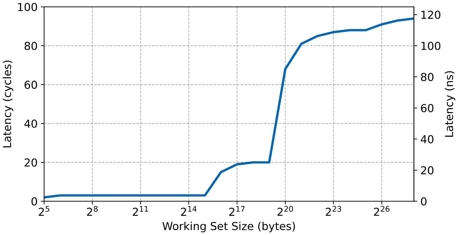
The latency results are the most interesting in this case. It clearly shows three plateaus with the first one being very close to a single cycle access (corresponding to the time needed to access the L1 cache). Note that the Cortex-A9 has a single cycle access latency to the L1 cache and a pipelined read instruction can also be executed in a single cycle. However, a little bit of measurement overhead is left in the test which means that access latency is measures at around 3 or 4 cycles. At around the 64 KiB mark, we start seeing a second plateau. Since the L1 cache is 64 KiB after that point, the working set doesn’t fit within the L1 cache which means that the test must now access the L2 cache which takes about 20 cycles. Finally, once the working set doesn’t fit into the L2 cache the test starts measuring the DDR memory access latency which, in this configuration, is about 88 CPU cycles.
It’s also possible to notice a fourth plateau in the latency results. This is the Translation Lookaside Buffer running out of space. The TLB is split into two levels on the Cortex-A9. Two separate instruction and data micro-TLB and a unified TLB. On the Zynq the micro TLB are configured with 32 entries while the main TLB is 128 entries. What we see in the results is the data micro-TLB running out of entry. In this test the page table is configured to use 1 MiB pages, which means that the micro-TLB runs out of place when the working set goes over 32 MiB.
Finally, on the bandwidth side of things, the maximum sustained memory bandwidths of the L1 and L2 caches are higher than the main memory. And although the L2 cache memory takes longer to access, the read and write bandwidths are very similar. In practice, and for usual access patterns, this is mostly due to pipelining within the Cortex-A9. In this case, with the access pattern being sequential, the read bandwidth is also helped by the automatic prefetch from the L1 cache.
On- Chip RAM and FPGA Bandwidth and Latency
Contrary to the previous section where the DDR memory was mapped as normal cacheable memory, in this section, the OCRAM and FPGA are mapped as non-cacheable device memory. First, this is a common configuration for those memory regions, and second, since the memory regions used in the test would fit into the L2 cache, performing the same test with those regions as cacheable memory would only benchmark the L1 and L2 caches and not the targeted memory itself.
OCRAM
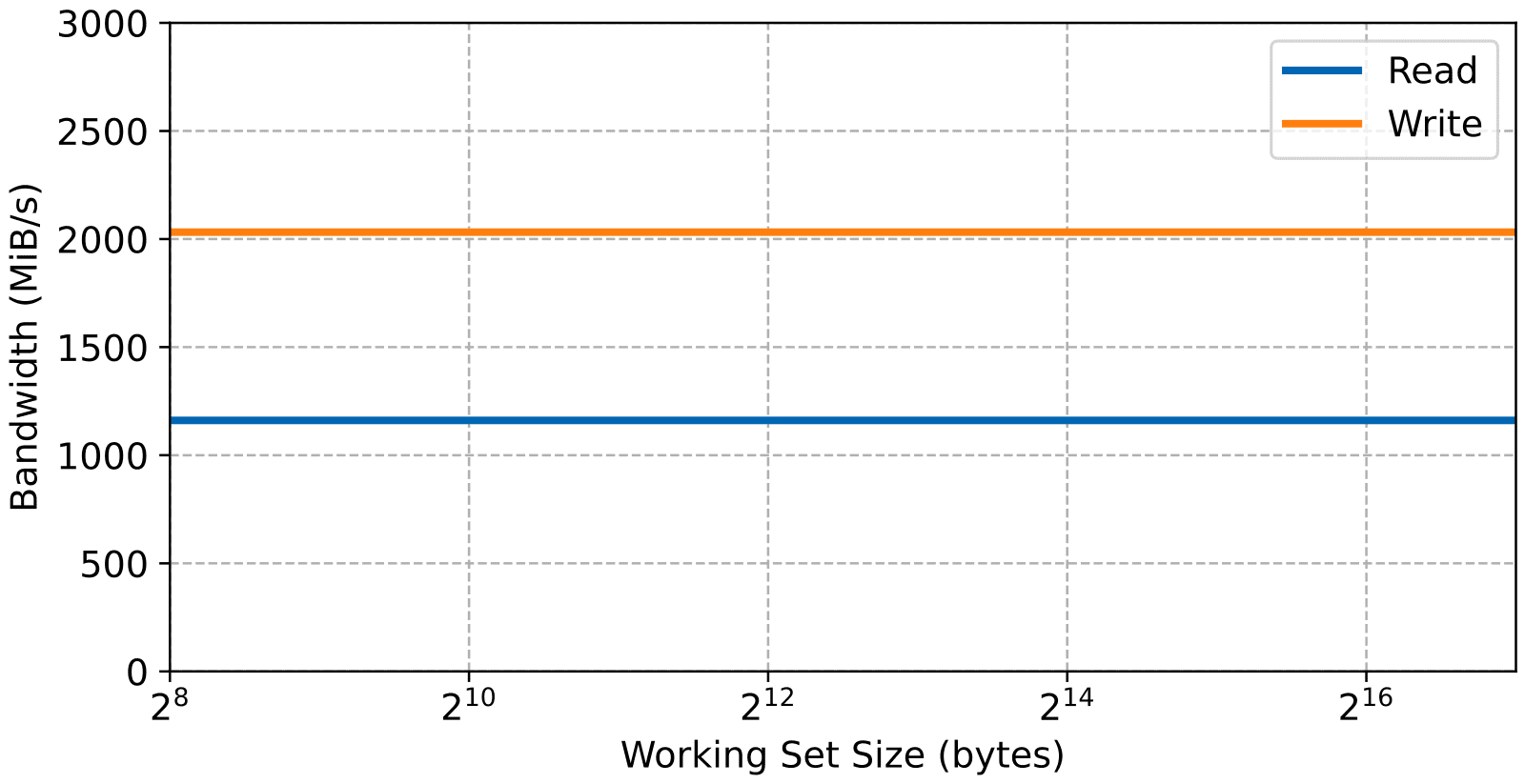
Let’s start with the on-chip RAM with the read and write bandwidth results below.
And now the read access latency, note that both figures only go up to a working set size of 128 kiB due to the size of the ocram.
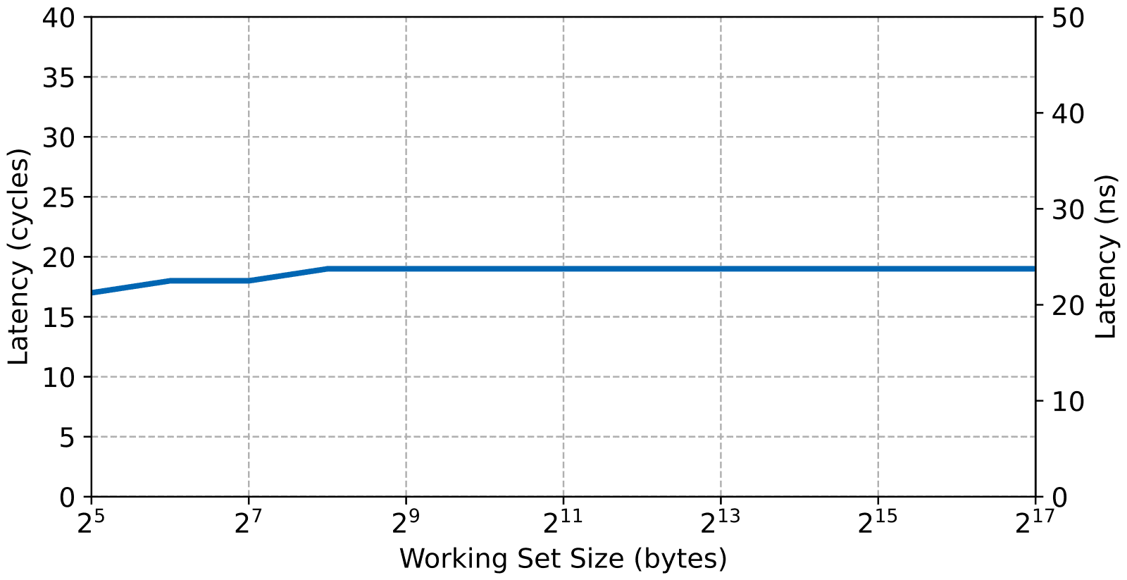
First and most obviously, since there’s no intermediary cache involved, the bandwidth and latency is mostly independent of the working set size. The next thing of note is that the OCRAM latency is about the same as the L2 cache, around 20 CPU cycles. Again, this is expected since the OCRAM is connected at the same level within the memory hierarchy. Finally, since the OCRAM is mapped as device memory, the read bandwidth is considerably lower as the CPU must wait for the read data without any help from automatic prefetching. On the other hand, writes are still posted so the access latency doesn’t affect them as much.
FPGA AXI Block RAM
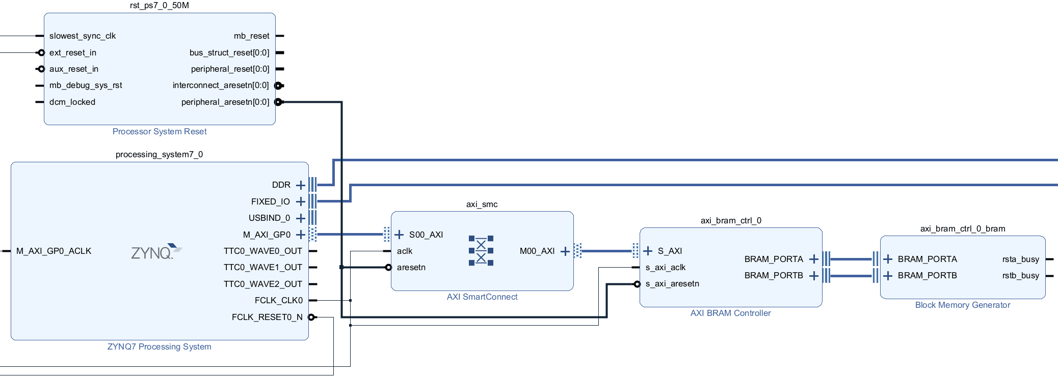
For this test, a single instance of the AXI BRAM Controller was instantiated within the FPGA. This is shown in the next figure. The controller is assigned a 256 KiB BRAM region and is connected to the AXI GP port through an SMC interconnect. The controller “Read Command Optimization” option is also enabled. Note that it’s also possible to connect the controller directly since there’s only one slave attached to the master port but that would reduce the maximum possible bus frequency and would be unusual in practice. For this test the bus frequency was set to the maximum possible of 250 MHz.
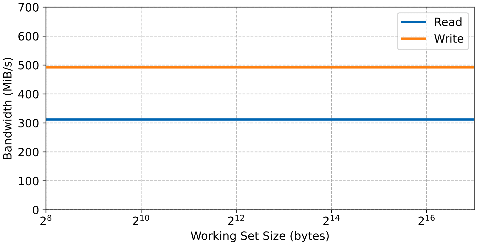
Here’s the measured memory bandwidth for this configuration.
And now the read access latency to the AXI BRAM.
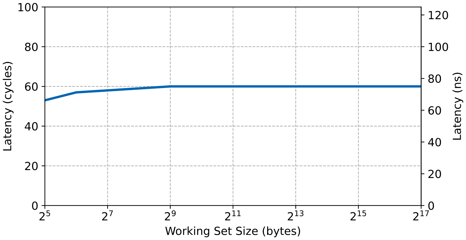
The BRAM being connected through a 32-bit bus and without caching, the bandwidth is obviously lower than all the results shown up to now. The latency, however, isn’t bad (around 60 cycles) which is faster than the external DRAM’s 88 cycles. On a lightly loaded system, this makes the FPGA access very quick, which is useful for real-time systems. Obviously, the latency will go up if a more complicated interconnect is instantiated in the FPGA to handle more than one slave. Also, bus contention in a real application could increase the jitter.
Memory Bandwidth and Latency Recap
Here’s a table that summarizes all the memory bandwidth and latency results.
| Read BW (MiB/s) | Write BW (MiB/s) | Read Latency (ns) | |
|---|---|---|---|
| L1 Cache | 2868 | 2786 | 4 |
| L2 Cache | 903 | 2765 | 31 |
| DDR SDRAM | 656 | 2046 | 88 |
| OCRAM | 1161 | 2032 | 29 |
| AXI BRAM (FPGA) | 312 | 492 | 93 |
From looking at the summary table, it’s clear that the farther the memory the longer the latency and usually the lower the bandwidth. The FPGA however, has lower access latency than the external DDR memory but lower bandwidth due to the width and speed of the AXI General Purpose bus.
Interrupt Latency
A discussion on bare-metal performance wouldn’t be complete without some words on interrupt latency. Interrupt latency, however, can be widely affected by the state of the cache and the application behaviour. For a longer discussion on the subject see our article on the Cortex-A9 interrupt latency. Also the interrupt latency depends on the interrupt handling code. In this test, we use the default BASEplatform interrupt handlers for a bare-metal configuration without saving the SIMD/VFP registers at interrupt entry. The result is a best-case interrupt latency, assuming everything is well cached, of 152 cycles or 190 ns at 800 MHz.
Conclusion
This is it for our bare-metal benchmarks of the Xilinx Zynq-7000. In this article we went over the synthetic CPU performance, memory access and latency for the L1 and L2 cache, on-chip ram, FPGA and external DDR memory as well as measured the typical interrupt latency. These values will serve as a baseline for a future article on the Zynq UltraScale+ MPSoC. Stay tuned!
If you have any questions or comments please do not hesitate to contact us.