In this article, we discuss the impact of real-time requirements on embedded file system performances and RAM usage. We show how to calculate the amount of buffering needed to absorb a hypothetical sequence of write accesses of varying duration. We show how RAM usage, write access time and average throughput are interdependent under our real-time assumption. In particular, we show how a higher peak access time (or a longer sequence of higher than average access times) requires either more RAM or a lower input rate, or a combination of both. Finally, we discuss how SD card and raw NAND flash compare in terms of access time and give guidelines for selecting the best option based on performance requirements and available memory, focusing on memory-constrained embedded systems.
Calculating Buffering RAM Usage for a Known Sequence of Access Times
Before we calculate anything, let’s first define what we mean by real-time requirements. For this article, we simply mean that the input data rate is fixed and that data loss is not allowed. Typical examples of fixed input rates are sensors with a constant sampling rate or logging information recorded at a given interval. A counter-example would be a communication link with some sort of throttling mechanism.
Now, consider a simple scenario where \(S\) bytes of some input data must be recorded at a fixed rate \(\omega_I\) on a non-volatile storage device of some sort. The storage stack as a whole (including the storage device, the file system and other related software) is such that the access duration varies from one access to the next. Letting \(\delta_k\) be the duration of the \(k^\textrm{th}\) access, the amount \(b_k\) of input data that must be buffered for the \(k^\textrm{th}\) access alone is
\(b_k = \delta_k \omega_I – S \quad . \tag {1}\)Simply put, that’s the difference between what comes in and what goes out. When the access time exceeds the input period (\(\omega_I^{-1}\)), \(b_k\) is positive and input data must be buffered. When the access time is lower than the input period, \(b_k\) is negative and whatever time is left after storing the current data can be used to empty the input buffer, effectively catching up with newly arriving data.
Assuming that we know the initial amount of buffered data, \(B_0\), the amount of buffered data after \(k\) accesses, \(B_k\), can be recursively calculated like so:
\(B_k = \textrm{max}(0, B_{k-1} + \delta_k \omega_I – S) \quad . \tag {2}\)Notice the use of the \(\textrm{max()}\) function and the recursive expression instead of a simpler summation. These are needed as the cumulated amount of buffered data cannot be less than 0.
Equation 2 expresses the fact that, under real-time constraints (fixed input period and no data loss) the latency requirement can only be relaxed at the expense of a lower input rate or a larger buffer size, or a combination of both.
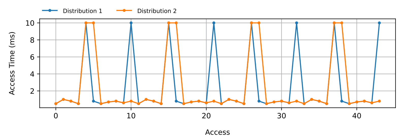
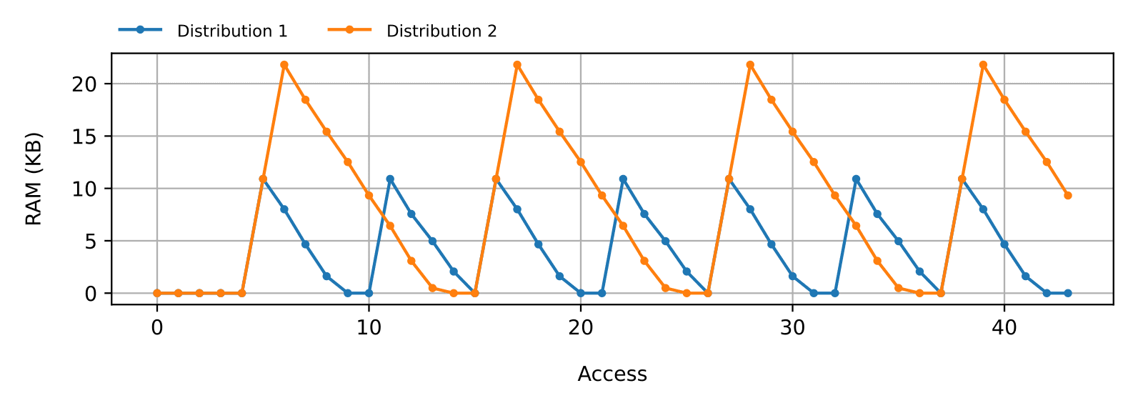
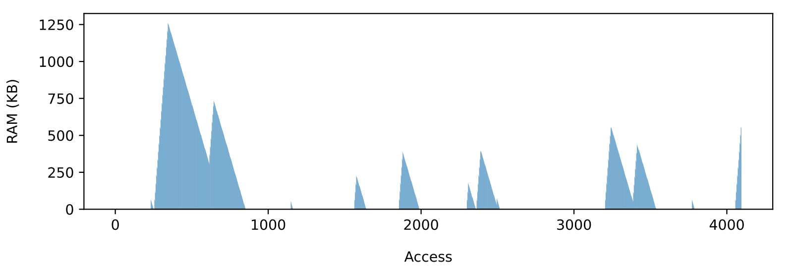
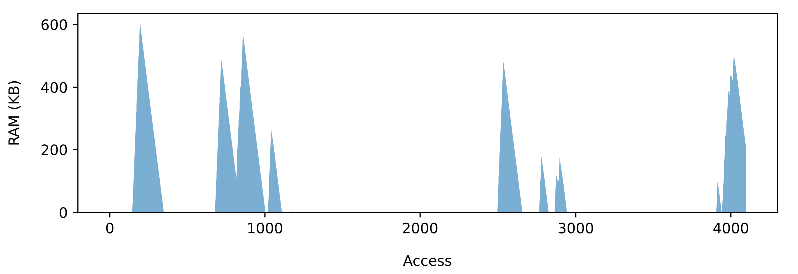
Notice that the order in which the individual access duration appears significantly impacts the peak RAM usage. To illustrate this, consider two hypothetical devices with two similar access time distributions (Figure 1). Both have the same maximum as well as the same total number of maxima. The only difference is where (and how far apart) the maxima are located. Notice how, in the second distribution, two consecutive peaks make for double the RAM usage of the first distribution (Figure 2). We can see how the peak RAM usage can vastly change even though the peak access time remains the same.
Managing Latency with SD/MMC
As discussed in a previous article, there are wide variations in overall performances across individual SD cards (the same goes for eMMC), and manufacturers do not usually provide detailed access time characterization, let alone any sort of timing guarantees.
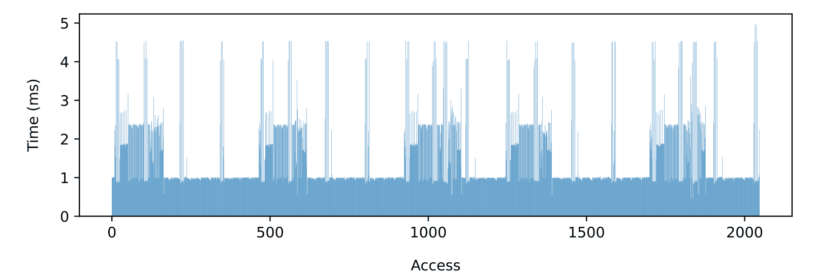
The SD card specification does include maximum duration, although it does not exclude or limit long sequences of maximum access time. The maximum busy time between blocks for a multi-block write operation, for instance, is 250 milliseconds which means a maximum duration of 2 seconds for a 4 KiB access. Fortunately, high-quality industrial SD cards can do better than the specification (Figure 3)
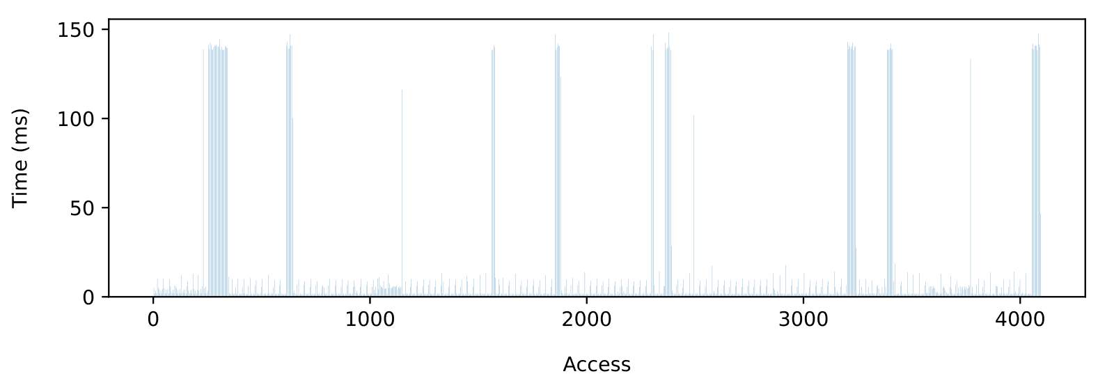
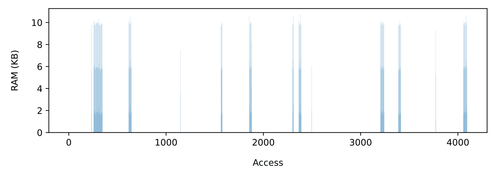
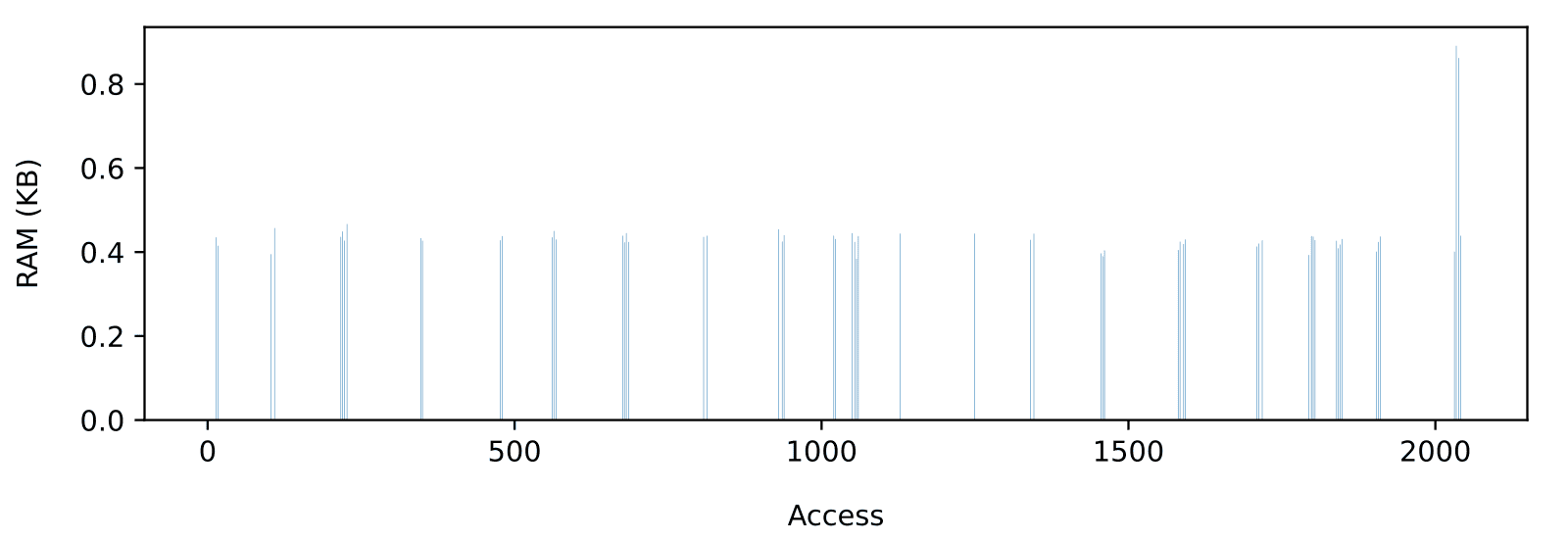
Regardless of the SD card, performances and RAM usage must be carefully balanced. To illustrate how the required amount of buffering grows with the input rate, consider the RAM usage for the sequence shown in Figure 3. Let’s assume 100 KB/s (Figure 4) and a 500 KB/s (Figure 5) input rate. The increase in peak RAM usage is dramatic, going roughly from 10 KB to 1 MB. Note that 500KB/s is much lower than the measured 1.5MB/s average throughput, which shows how achieving the full-throughput potential of the card without data loss is only possible on larger embedded systems with lots of RAM available.
The required amount of buffering also varies from one card to another given the same input requirements. Consider the RAM usage recorded for the longest access sequence obtained on a 16 GiB Sandisk Ultra card (Figure 6). That card requires 60 times more RAM than the Swissbit to accommodate a 100KB/s input rate without data loss.
In any case, empirical access time characterization on SD card or other managed flash devices is hazardous because timing depends on a variety of factors beyond the application’s control (like the exact access pattern produced by the file system at the device level) or even beyond the file system’s control, like the internal state of the built-in flash controller.
Empirical device characterization can mostly be avoided by using managed flash devices where they most make sense, usually in one of the following three scenarios:
- No real-time constraints. If data loss is allowed or the input rate can vary, then access latency is much less of an issue. In that case, very high input rates can be accommodated with little to no buffering.
- Real-time constraints on larger MCU (with external RAM). If RAM is not an issue, buffering can be increased such as to absorb any anticipated worst case, and provide the highest possible throughput while meeting real-time requirements.
- Real-time constraints on small MCU with low throughput requirements. With limited RAM available, throughput must be sacrificed, which can either be a very sensible choice or a complete disaster depending on the application. For real-time applications with high write throughput requirements (>100KB/s) and limited RAM, raw NAND should be considered (see next section). Otherwise, SD/MMC could be the right choice. Using the SD specification as a reference for a quick calculation, no buffering is needed as long as the input rate does not exceed 2KB/s (512 bytes / 250 ms). Of course that mark could be improved based on manufacturer data or experimental device characterization, but with anything less than a few hundreds of kilobytes in dedicated buffering memory, throughput much lower than the average is to be expected.
A Better Real-Time Alternative for memory-constrained Systems
For real-time applications with modest amounts of RAM but higher throughput requirements (> 100KiB/s), a raw NAND device paired with a real-time flash file system like TSFS is a great alternative to SD card or eMMC.
Let’s discuss the device first. For the smallest embedded systems, this would likely be SLC NAND with a QSPI interface, while more capable, industrial-grade MCUs could benefit from performance enhancements like plane parallelism, or from increased density with an SLC or MLC parallel device. Either way, the worst-case access time is determined by the maximum block erase time provided by the manufacturer. This is a crucial benefit from a real-time perspective, not only because erase time on NAND flash is relatively low (the Micron MT29F1G01 QSPI SLC NAND has a specified maximum block erase time of 10 ms) but, more crucially, because the file system gets to decide exactly when access time peaks occur. This is how TSFS, for instance, can provide strict timing guarantees.
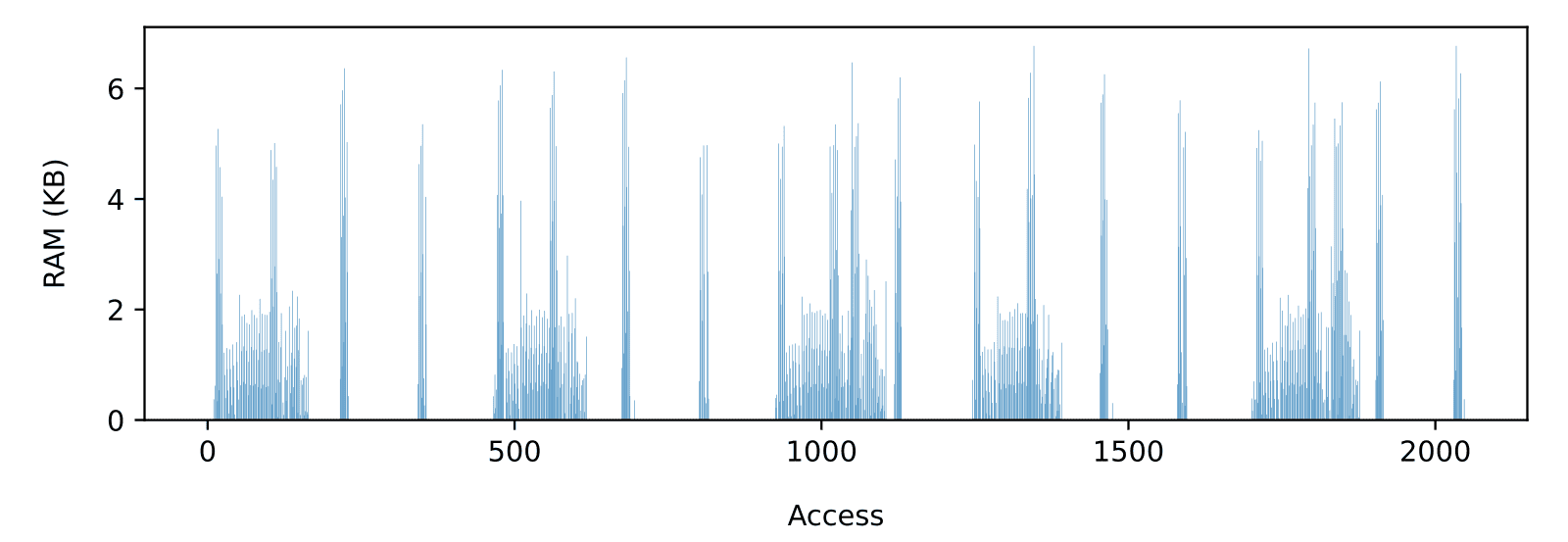
Comparing TSFS file-level access times on the Micron MT29F1G01 SLC QSPI NAND (Figure 7) with previously discussed raw SD card access times (Figure 3), we can clearly see why raw NAND is a better solution for real-time applications with strict memory constraints. On a high-quality industrial-grade SD card, 1 MiB of RAM was needed to reach a 500KB/s average throughput (Figure 5). That is, not including the added impact of a potential file system. By contrast, on the MT29F1G01, TSFS can accommodate an input rate of 500KB/s with no buffering at all, 1MB/s with less than 1 KiB (Figure 8), and 2MB/s (Figure 9) with less than 10 KiB while meeting real-time constraints.
Conclusion
Raw NAND flash is a great option for most small to medium embedded applications with real-time constraints. Paired with a real-time flash file system like TSFS, it provides high throughput with tight timing guarantees which makes it much easier to anticipate memory needs and set performance expectations early on in the design phase. Industrial SD cards and eMMCs still have their place, of course, where large amounts of data are stored and/or very high write throughput are required, although, in the presence of real-time constraints, RAM usage and performance must be carefully balanced.
As usual, thank you for reading. If you need advice on anything related to embedded storage or embedded systems in general, please feel free to contact us.