In the previous article from this series, we looked at the core performance of the Xilinx MicroBlaze soft core CPU in various configurations using the popular CoreMark benchmark. While CoreMark is good at measuring core CPU performance it is mostly transparent to memory performance since, it’s designed to run entirely out of the L1 cache. In this article, we will leave behind core performance to focus on the memory hierarchy. To be more precise memory bandwidth and access latency.
Note from the author:
This is one of the first articles inspired by readers’ feedback and questions. Going forward, I would like to write more articles answering questions received from readers. If you have any feedback or topics, you’d like to be covered do not hesitate to contact us by email at blog@jblopen.com.
You can also look forward to articles written by other members of the JBLopen team in the near future. If you want to be notified when these articles are published feel free to follow us on Linkedin, Twitter, Facebook, or your favourite RSS reader.
Measuring Memory Bandwidth and Latency
Measuring bandwidth and latency from the CPU can be a little bit tricky as the measurements are invariably affected by the access pattern used for benchmarking. This is especially true for CPU cores with automatic prefetch engine which can improve or worsen the measured bandwidth and latency. This article use the results of two custom benchmarks that are part of our BASEplatform test suite. The tests in question are designed to measure the maximum sustained read bandwidth as well as the read latency of a single word. The output of the tests are graphs of read bandwidth or latency versus the working set size.
Read Bandwidth
The first test repeatedly reads a region of memory using a hand-coded loop. The size of the region is called the working set and the read loop is repeated many thousand times to eliminate the effect of prefetching and stride detection. As an example here’s the read bandwidth vs working set size of the Xilinx Zynq-7000. The test was ran on the krtkl snickerdoodle using 400 MHz LPDDR2 and the Zynq running at 666 MHz.
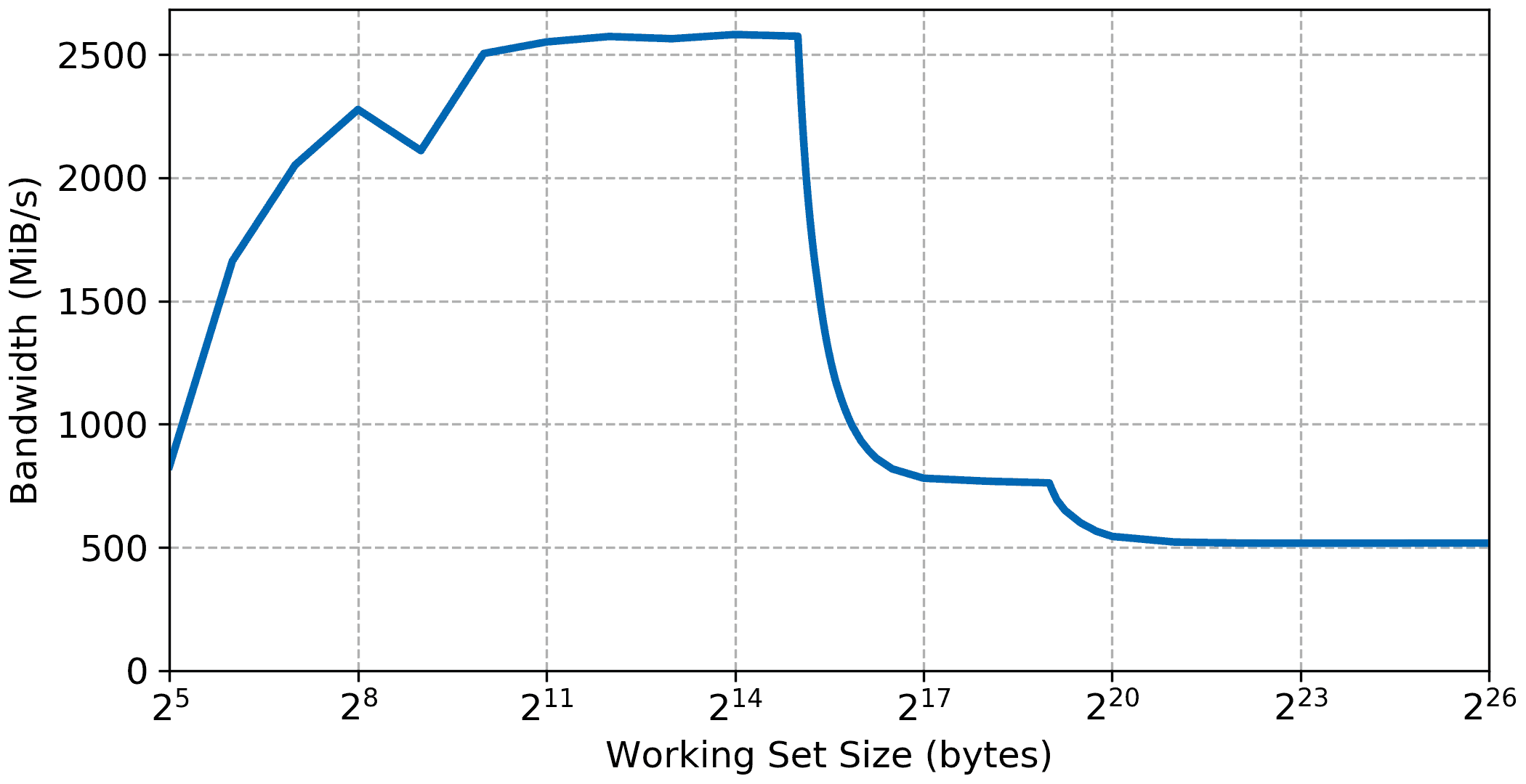
On a SoC with a multi-level cache hierarchy one can expect the graph to show various plateaus corresponding to where the working set fits in the memory hierarchy. Here we can clearly see the read bandwidth of the L1 & L2 cache and main DDR memory. The initial climb is due to the benchmarking overhead becoming inconsequential compared to the working set size, with measured performance nrealy reaching 2600 MiB/s. This initial performance plateau corresponds to the L1 read performance and stays up to a working set size of 32 KiB which matches the size of the L1 cache on the Cortex-A9 of the Zynq-7000. The second step settles briefly to a slightly lower bandwidth of about 850 MiB/s up to a working set of 128 KiB/s this time the size of the L2 cache. Finally, the bandwidth settles to the sustained read bandwidth when reading from the external DDR memory at 518 MiB/s.
Read Access Latency
Memory access latency is somewhat harder to measure. The method used in this article is similar to the technique used in the venerable LMBENCH utility. A word is read from memory which contains the address of the next word to read. This effectively measures the time it takes to perform back-to-back memory loads were the result must be available before the next memory access can be performed. In an attempt to defeat automatic prefetchers LMBENCH tries to use stride and backward accesses which aren’t always sufficient. The BASEplatform randomizes the pointer’s targets to make them difficult to prefetch.
For example, here are the results for the same Zynq-7000 platform:
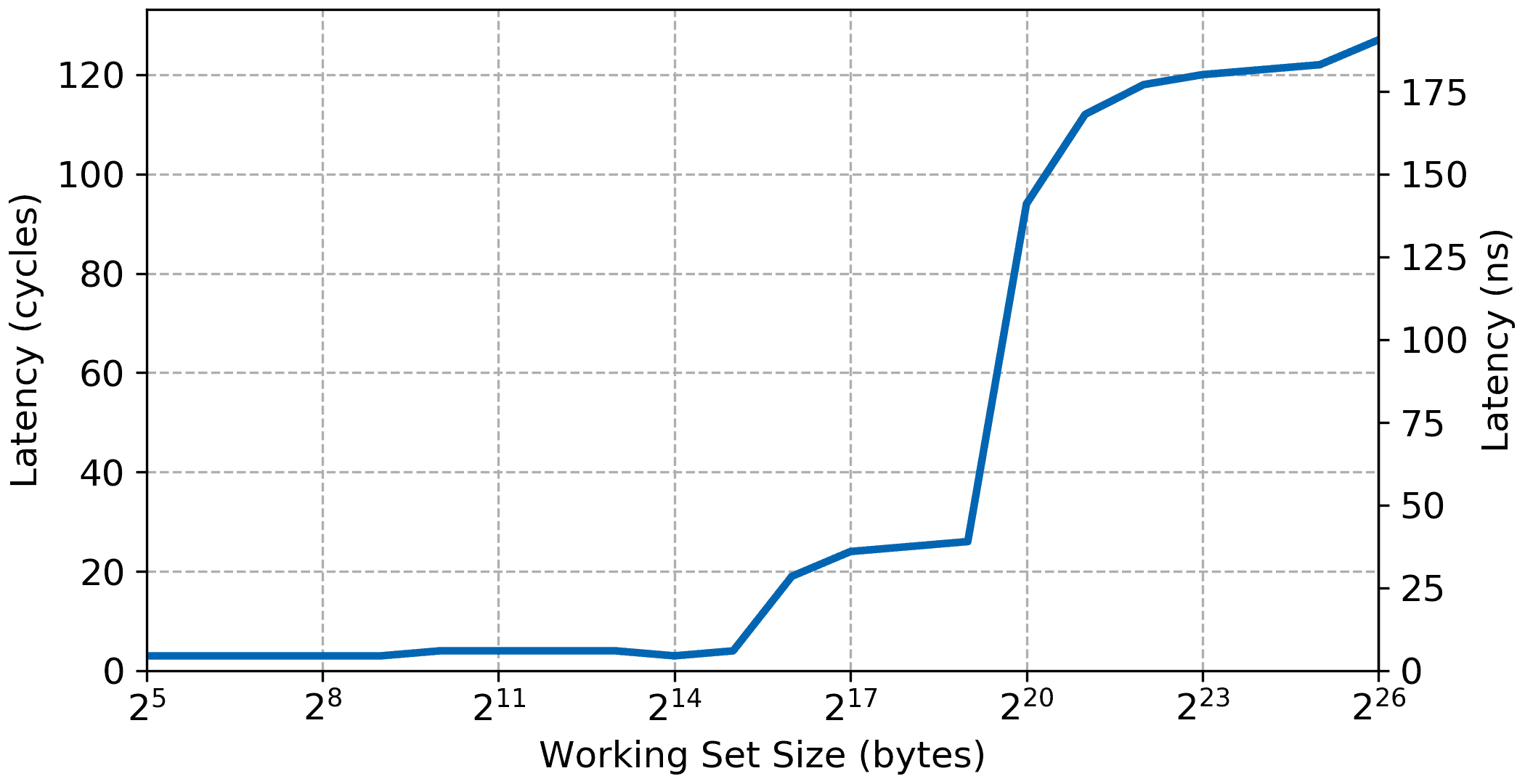
The overall shape of the latency curve is the inverse of the bandwidth curve. The early values for small working set up to 32 KiB are very low, around 3 cycles which includes the back to back read and measurement overhead. Latency for the L2 cache is about 25 cycles up to the size of the L2 cache (512 KiB. And finally the access latency for the external DDR is around 120 cycles. Under different conditions the test could show a fourth plateau once the working set gets larger than what can be mapped in the TLB but the Zynq-7000 has a rather large TLB so this test doesn’t show the effect of the TLB on the access latency.
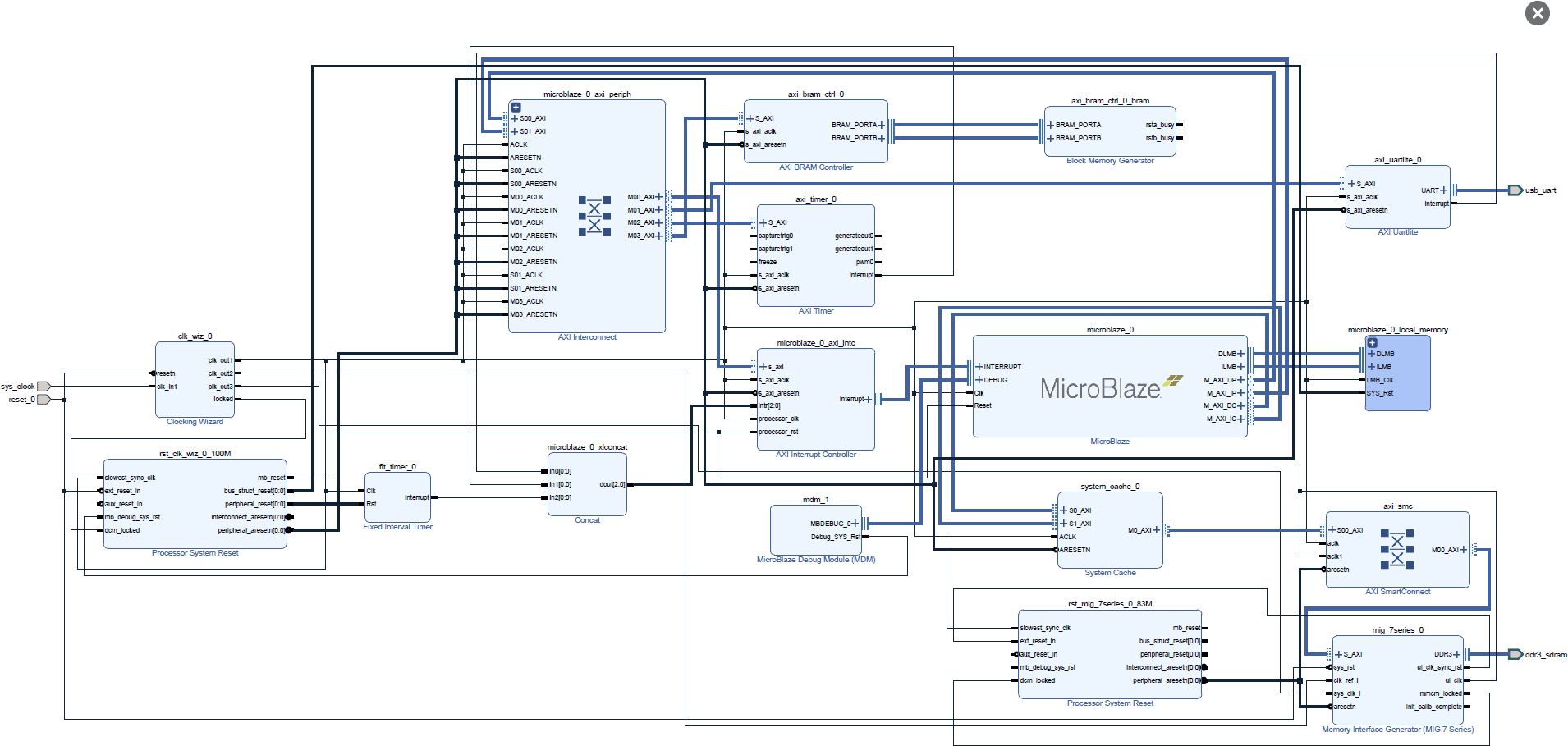
MicroBlaze Configuration
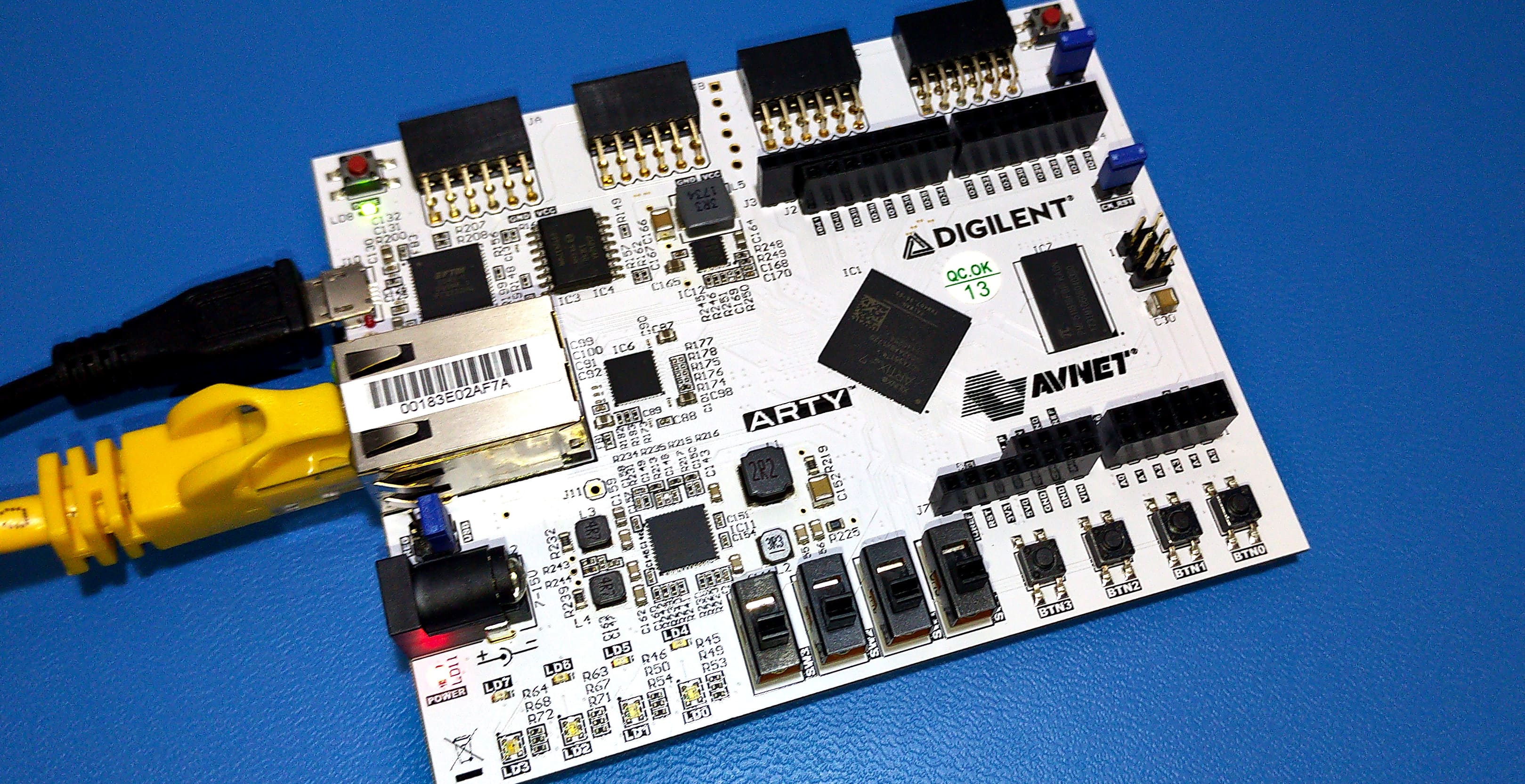
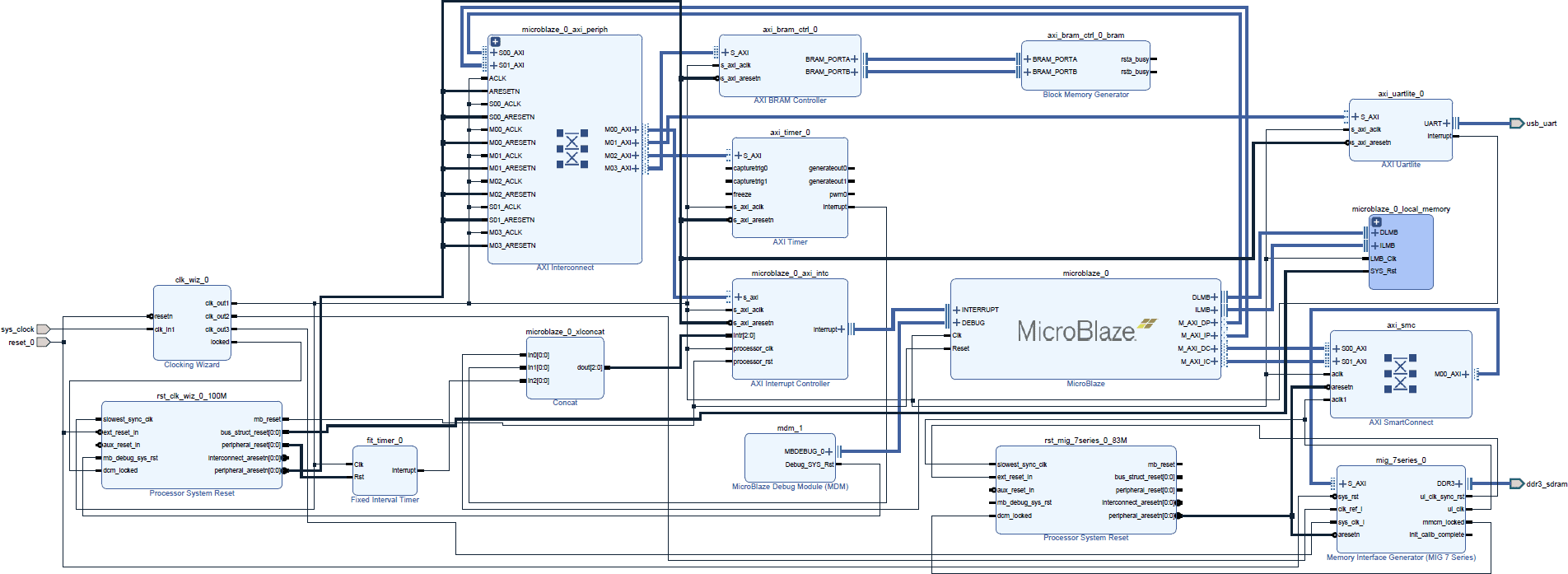
The MicroBlaze configuration for this article is the same as the previous article using the Digilent Arty7-35.
The MicroBlaze is clocked at 100 MHz MicroBlaze connected to various memories for benchmarking. When using the external DDR memory the MIG IP block is clocked at 166 Mhz which means that the AXI interface is clocked at 83 Mhz. This adds a little bit of latency due to the synchronization stage required in the AXI bridge but enables the MicroBlaze to run at 100 MHz.
Benchmark Results
Local Memory
Similarly to previous articles we’ll look at different memory hierarchy starting with local memory. When running from local memory, the MicroBlaze can perform a memory access in a single cycle except when using the frequency optimization implementation. Other than the benchmark overhead we should expect a single cycle memory access. For a 32-bit MicroBlaze implementation, the memory bandwidth from local memory can theoretically reach 4 times the CPU frequency, or roughly 381 MiB/s.
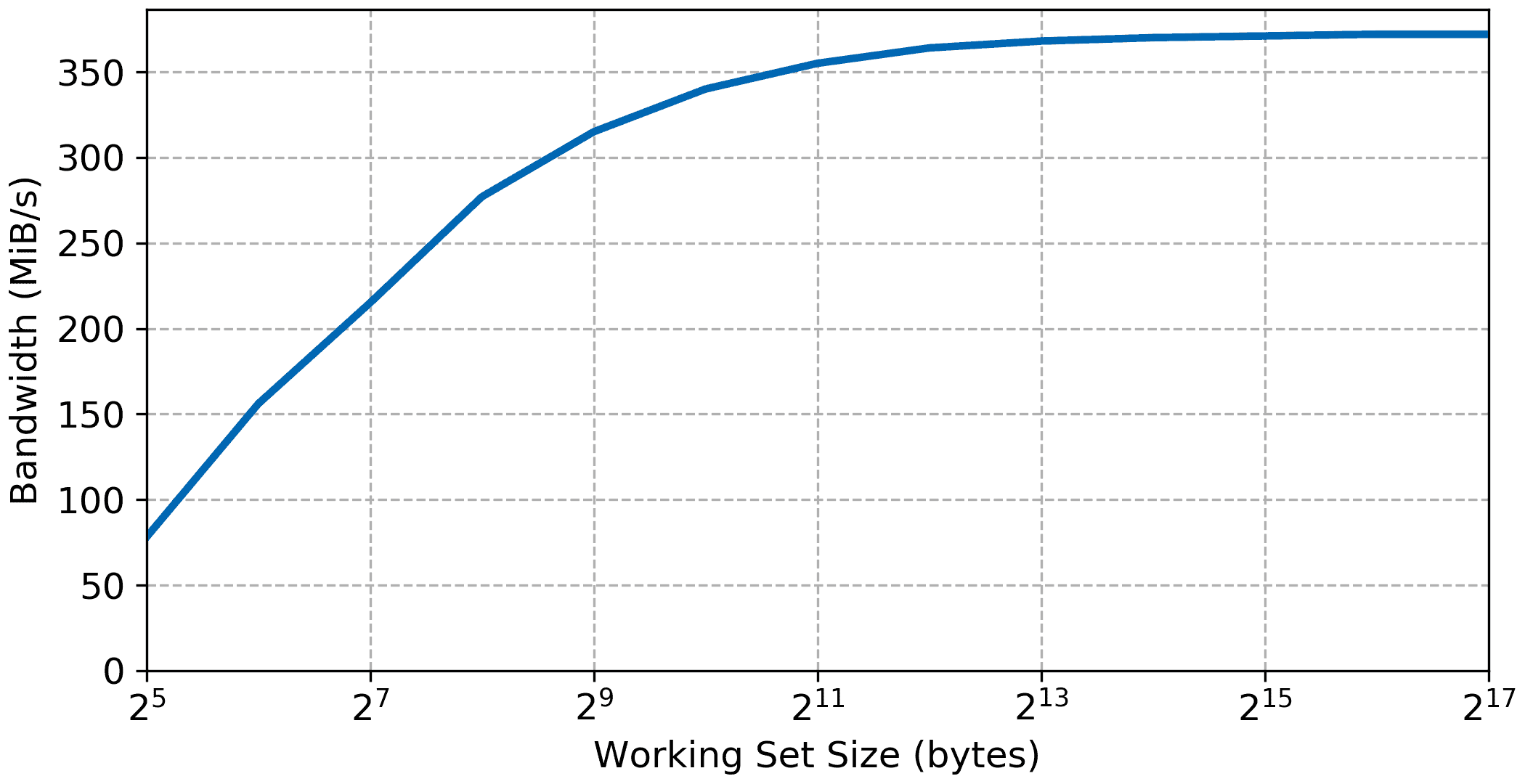
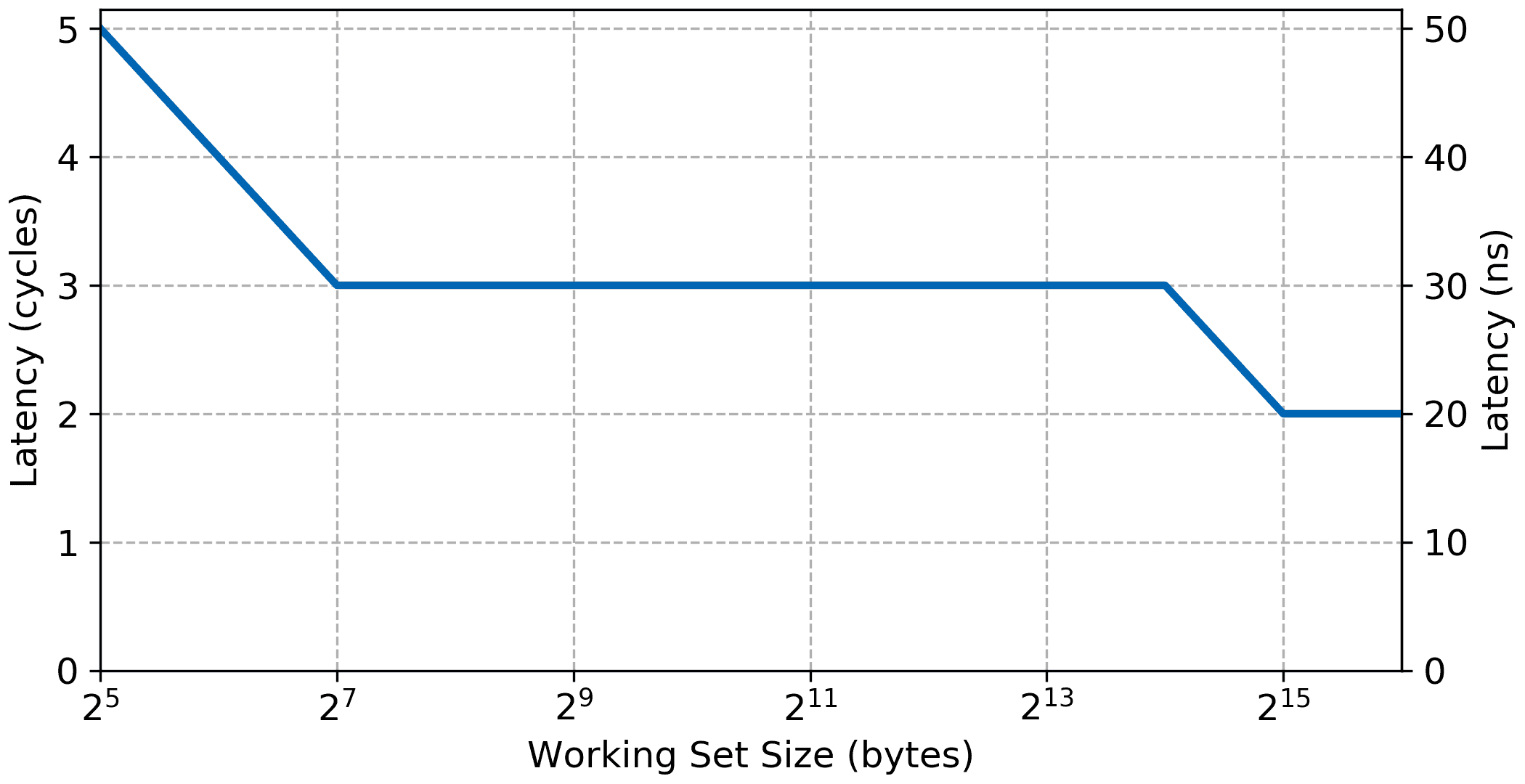
The bandwidth curve shows the initial benchmarking overhead but reaches close to the expected value with a measured bandwidth of 372 MiB/s. Same for the read access latency being very low around two cycles for a back-to-back access including the benchmark overhead. Since this is running from local memory and there is no cache we should not expect any plateaus in the graphs.
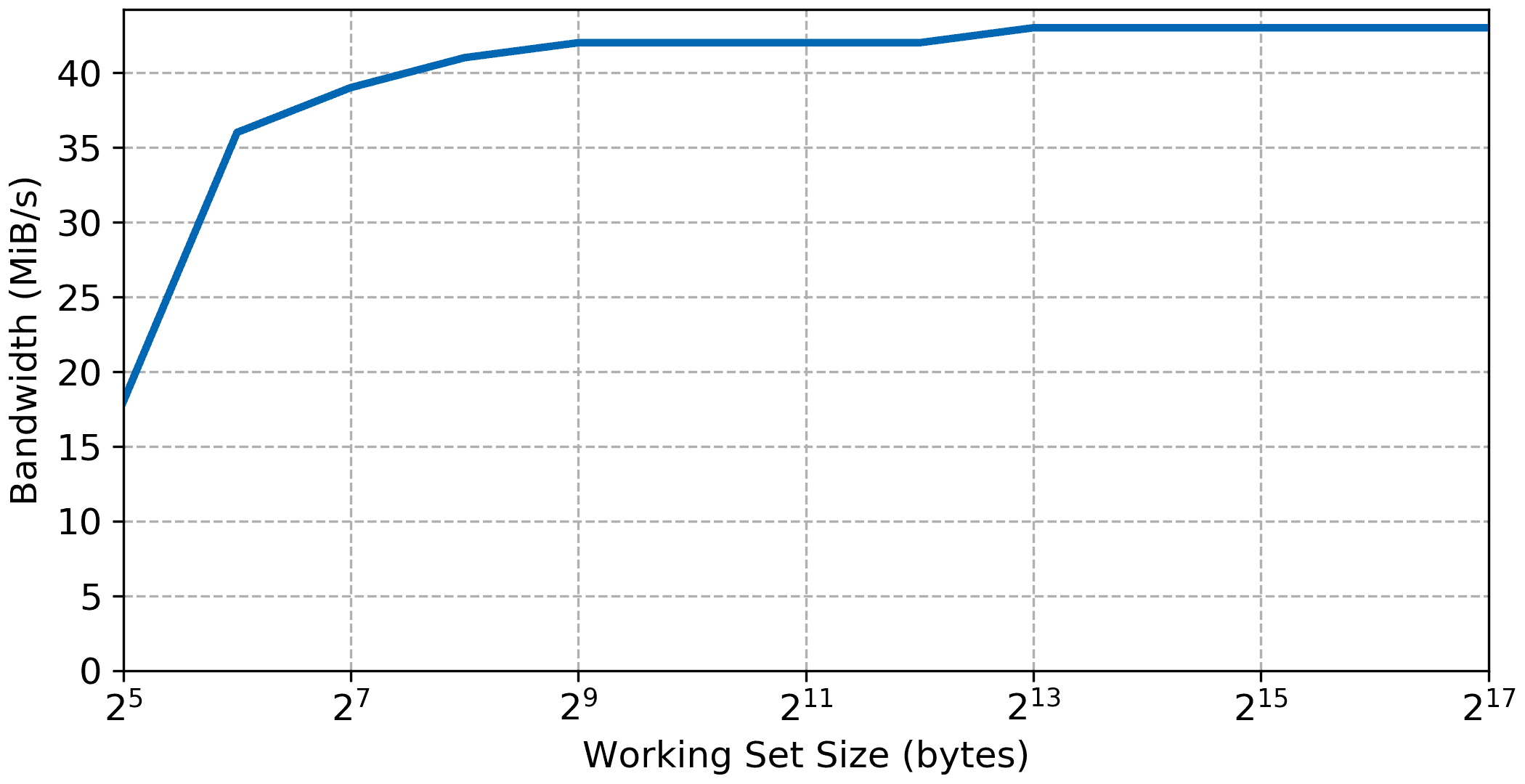
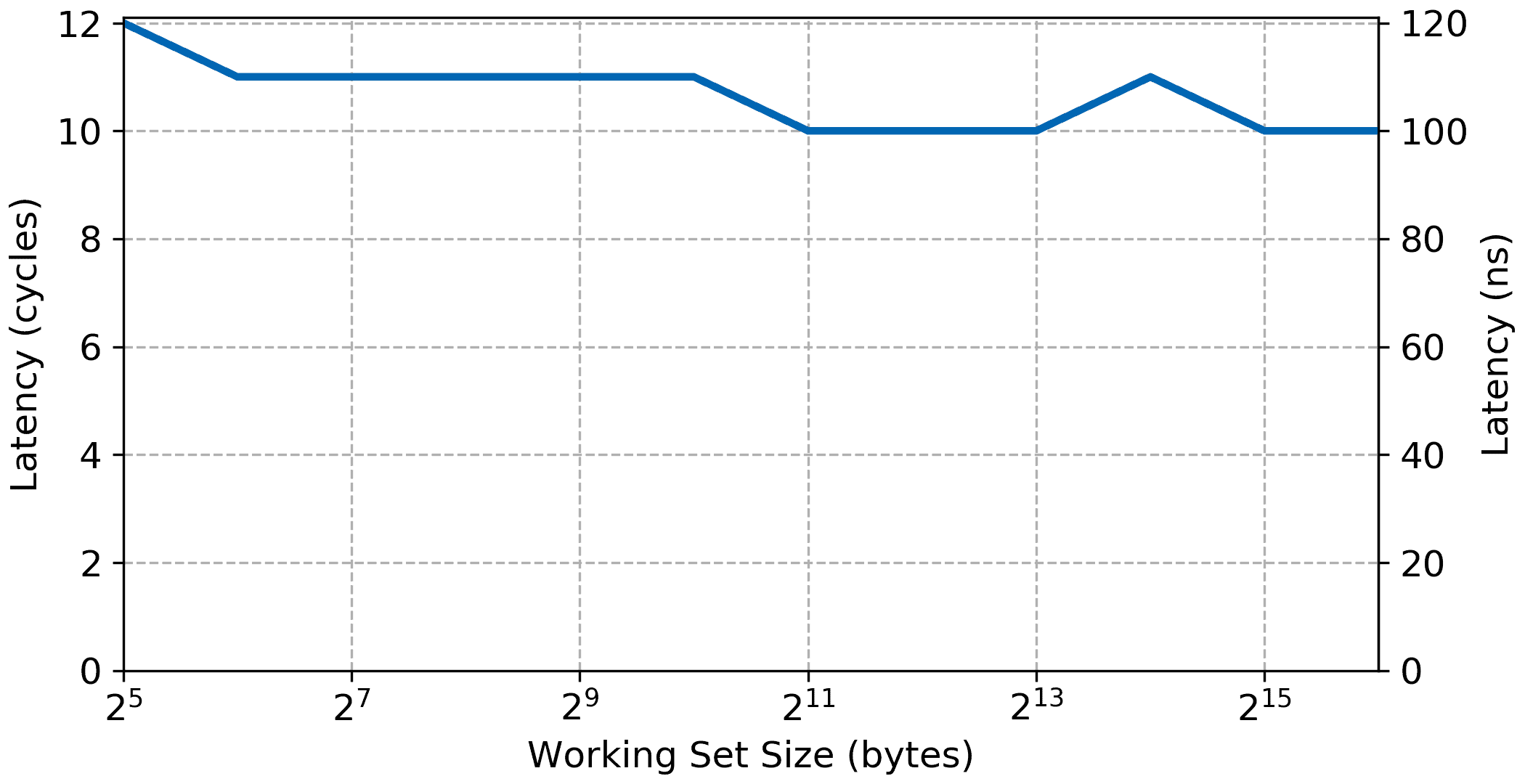
AXI Block RAM
AXI block ram connected through the peripheral data port does not benefit from the cache nor from the low latency access of the local memory bus(LMB). As such we should not expect the bandwidth and latency to be as good, but similarly to the local memory there shouldn’t be any significant steps in the data.
External DDR Memory
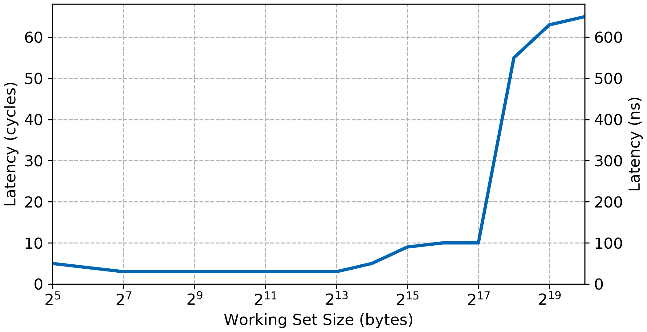
Things get more interesting once we look at external RAM. Here the cache effect should be visible while the maximum latency once the working set gets larger than the internal cache should be considerable.
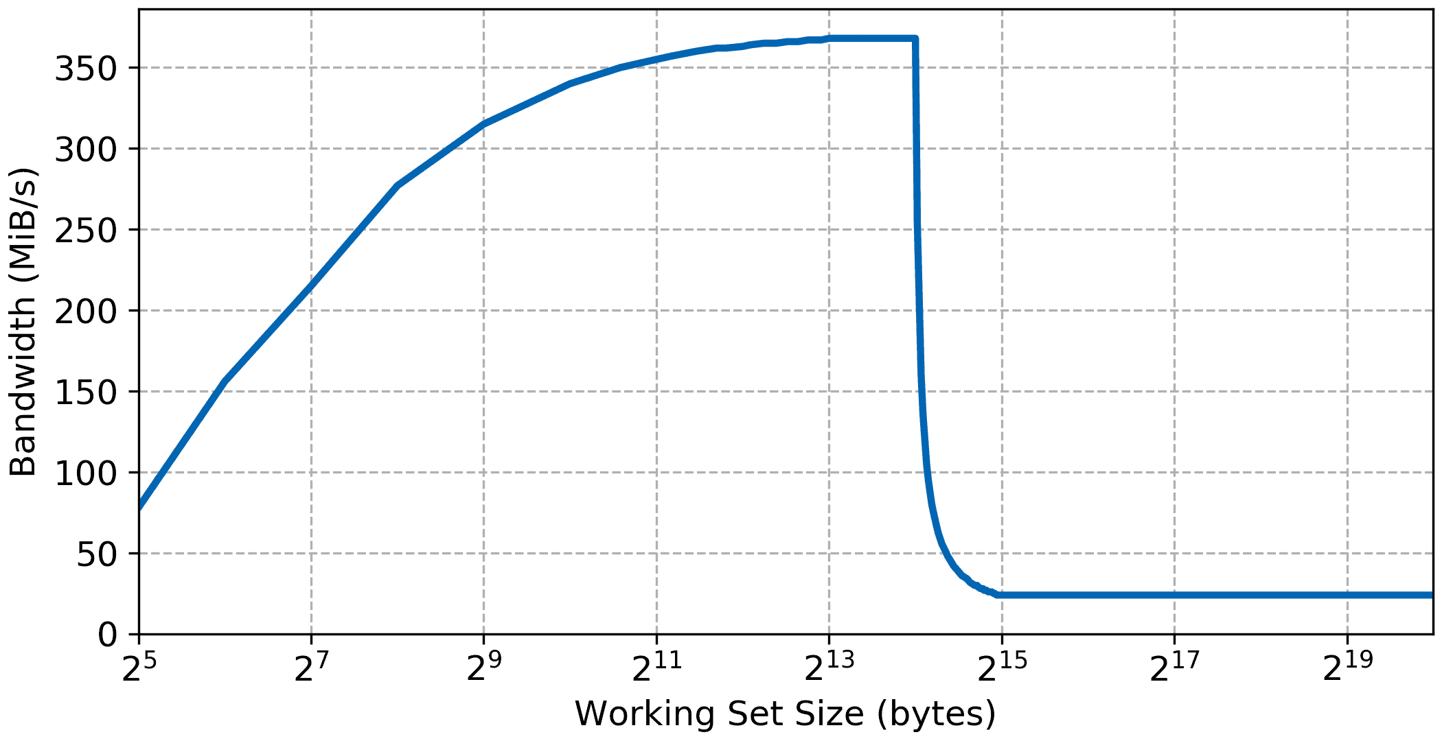
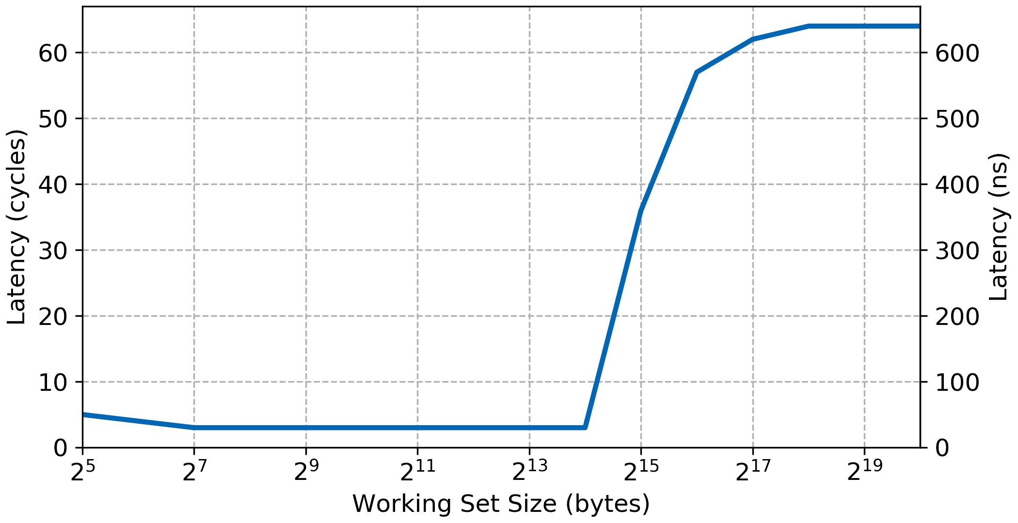
Like all the other the initial curve is due to the measurement overhead. The bandwidth increases to the maximum L1 bandwidth of 368 MiB/s very similar to the local memory results. Latency is also very low for small working set showing that the MicroBlaze can perform single cycle memory access from cache, again similar to the result when running from local memory.
However, once the working set gets over the size of the L1 cache, 16 KiB the bandwidth sharply decreases while the access latency increases. Access latency goes up to around 64 cycles and bandwidth settles at 24 MiB/s.
What About an L2 Cache
The MicroBlaze will usually have a single L1 Harvard cache split between the data and instruction sides. However within Vivado there is a system cache IP which can be used as an L2 cache. By itself it would be a bit wasteful but while being here let’s look at the performances with an L2 cache added.
The System Cache used in this test has a 128 KiB size with 16 bytes line length. Contrary to the MicroBlaze Cache, the System Cache is not direct mapped but has a configurable associativity of 2 or 4. The associativity was set to 4 in this test although it should have a minimal impact on the result of these synthetic benchmarks.
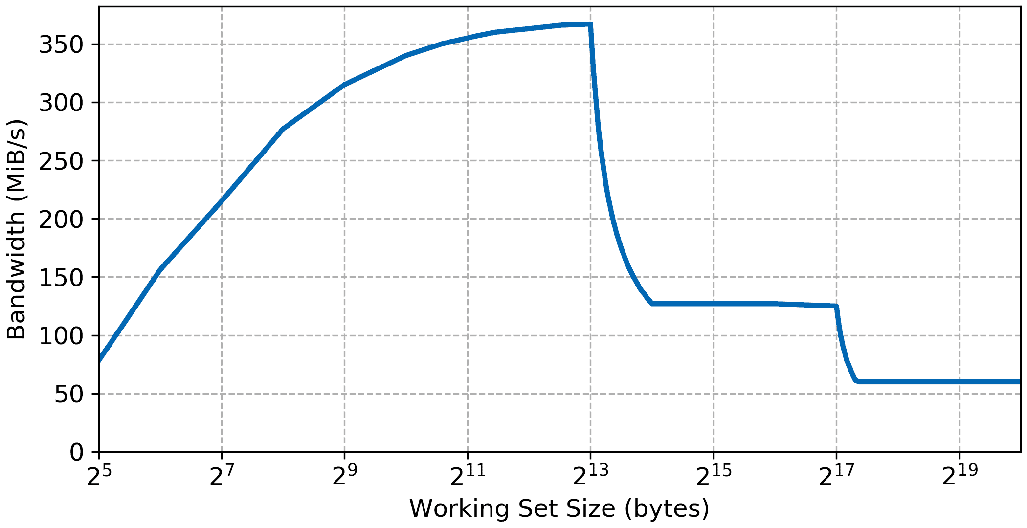
With the addition of the L2 cache a third step appears in the bandwidth and latency graph, basically improving performance for working set between the size of the L1 cache now up to the size of the L2 cache, i.e., 128 KiB. The data possibly show a slight increase in DDR memory access latency, around 1 cycle but overall the System Cache appears to have a very low access latency in itself.
I hope you enjoyed part 2 of this series. The next article on the MicroBlaze performance will deal with more detailed benchmarks of the impact of some advanced MicroBlaze configuration on RTOS performance.
Click here to read Part 1 of this article series about the MicroBlaze core performance or here to learn about configuring a MicroBlaze for your application.
Questions or comments?
Do not hesitate to contact us at blog@jblopen.com. Your questions, comments and, suggestions are appreciated.