This article is the first of a series on flash file systems performance analysis. In this particular article, we show how the maximum average write throughput on a given flash device varies with the amount of stored data. We provide a simple performance model that can be used for setting realistic performance expectations, comparing file system performances, and questioning application requirements with minimal assumptions regarding the actual workload or file system implementation.
The performance model that we develop in this article equally applies to all flash file systems or flash translation layers (FTL), including FTL found inside managed flash devices such as SD cards and eMMC chips. However, in the case of managed flash, we usually don’t know the actual capacity and raw throughput of the internal flash array, such that, in practice, our model (or any model) is of limited use. By contrast, applying our conclusions to raw flash devices is very straightforward, as you will see.
Copy-On-Write
Before we jump into the maths, we need to understand what we are working with. Flash memory is governed by specific restrictions as to how it can and cannot be accessed. When it comes to writing, it all basically boils down to this:
- You can only program (write) whole pages.
- You can only erase whole blocks.
- A single block contains many pages.
- A page must be erased before it can be programmed.
Given these restrictions, modifying the flash memory content is no trivial task. We know that the updated page must first be erased (property 4). But then, all other pages in that same block — some of which likely contain valid data — must also be erased (properties 2 and 3). One apparent solution is to load the whole block in RAM, modify the content, erase the block, and write the modified content back to its original location. This basic algorithm, however, suffers numerous flaws:
- RAM usage: erase blocks are commonly larger than 64 KiB — they can be as large as a few megabytes on higher density NAND — which is a lot of RAM for the average MCU.
- Performance: erasing a block takes quite a lot of time (a second or so for NOR flash), so one block erase per update will yield extremely poor write performances.
- Wear: a block can only be erased a limited number of times before it ceases to function properly. One block erase per update will drastically shorten the device lifetime.
- Fail Safety: a power failure (or any other untimely interruption) occurring between the block erase and the final write will result in the loss of the entire block’s content.
These flaws arise from one single, implicit (and unnecessary), requirement, which is that the data be modified while retaining its original location. Indeed, consider what happens if we remove that requirement.
If we allow the modified page to be written back to an alternate destination block, the above-mentioned problems simply dissolve. There is no need to erase the source block, so there is no need to move its content elsewhere, and no need to load its content in RAM either. Now, the source block will be erased at some later point, but not until the (out-of-place) update is completed, effectively preventing any data loss caused by a potential power failure. Write speed and life expectancy are significantly improved as well because erasing is only needed once the destination block is full — as opposed to once per individual update for the in-place approach.
But nothing comes for free and, in this particular case, the price to pay for all these improvements is increased complexity. Indeed, having pieces of data moving around all the time is not very convenient from a user’s perspective. Some sort of persistent addressing scheme must be provided so that any bit of stored data can easily be retrieved or modified at some later point in time. All that extra bookkeeping comes with its very own set of challenges and tradeoffs, but for now, we don’t need to worry about that.
The out-of-place update algorithm that we have just described is commonly referred to as copy-on-write. There are many benefits to using a copy-on-write strategy regardless of the storage media at hand, but in the case of flash memory, copy-on-write is practically unavoidable.
Garbage Collection
As updates are being performed through copy-on-write, the number of free blocks will decline until, eventually, no free blocks remain. At that point, the data distribution across the whole flash could look something like that represented in Figure 1, where gray areas represent valid data and white areas represent free space. Remember that, in the context of copy-on-write, space is freed when the corresponding data is updated and thus moved to some alternate location.
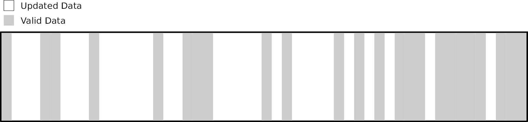
Once free blocks have been exhausted, the copy-on-write algorithm cannot continue nor recover: it has gone one step too far. Not because of the lack of free space (white areas), but rather because of the lack of empty erase blocks. Indeed, since the remaining free space is more or less evenly spread across all erase blocks, no block can be erased without also erasing valid data. This is where garbage collection comes in.
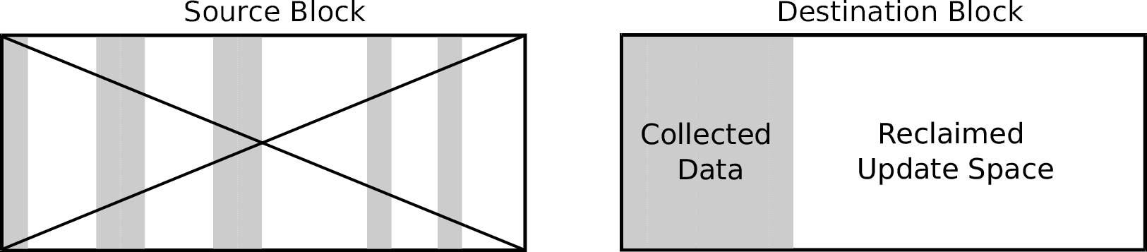
The garbage collection process is very straightforward, although producing an efficient implementation is not so easy. Garbage collection must start before all free blocks are exhausted (at least one free block must remain). It operates on one block at a time, copying all valid pages within that block (the source block) to one of the remaining free blocks (the destination block). Once all valid data has been moved, the source block can safely be erased.
Notice that the amount of free blocks remains the same after the process has completed, but the remaining space inside the destination block can now be used to accommodate further updates, as shown in Figure 2. Once the destination block is full, the garbage collection process is repeated using the previously freed block as the new destination.
Although garbage collection is a direct consequence of copy-on-write, the specific implementation that we describe here is not. In our implementation, a block is freed by moving the remaining bits of valid data to an alternate location. That is required on flash memory, but on devices supporting in-place updates, free space can simply be filled with subsequent updates — there is no need to move surrounding bits of valid data anywhere.
Write Throughput Estimation
So far, we have shown that copy-on-write and garbage collection are inevitable consequences of intrinsic flash properties and restrictions. Given the extra reading and writing that comes with garbage collection, we can start to appreciate its potential impact on write performances. In fact, we can already predict that increasing the amount of stored data will simultaneously increase the block collection frequency and the amount of reading/writing per collected block, suggesting a superlinear relation between the performance overhead and the fill level (i.e. the amount of stored data divided by the capacity).
To put that in numbers, consider a flash memory which content is continually updated at random, uniformly distributed positions. By the way, random writes are considered for two main reasons here. On one hand, embedded applications with mostly random workloads are not uncommon (e.g. databases). On the other hand, a purely random workload will usually yield the lowest performances (sequential accesses would yield the highest), providing a safe starting point for setting and questioning performance requirements without much assumption regarding the actual workload.
Back to our example, let \(m\) be the size of the memory and \(s\), the size of the dataset. Let’s further assume that all updates have the same size \(p\), which is also the page size. Given random accesses, the probability \(u\) for any given page to be selected for update is
and the probability \(v\) that the extent is still valid after \(n\) updates is
To achieve the highest possible write throughput, the block selected for garbage collection must be the one with the least amount of valid pages. In the case of random accesses, that block is always, statistically, the least recently programmed block (keep in mind how copy-on-write proceeds, filling one block after another). Under those conditions, the number \(n\) of updates that can be performed before the block currently being programmed is selected again for garbage collection is
where \(m/p\) is the total number of pages and \(1-v\) can be interpreted as the average proportion of a block used for new updates (as opposed to garbage collected data). Now, let \(l=s/m\) be the fill level and \(k=p/m\), the page-to-media size ratio. Combining equations 2 and 3, we have
When discussing random access performances, we usually imply that updates are small (much smaller than the whole device anyway), so we evaluate the limit when \(k\) approaches 0
Equation 5 is a non-algebraic equation, but it can still be solved for \(v\) using the Lambert \(W\) function (or product log function). Don’t worry if you are not familiar with the Lambert \(W\) function. If you want to learn about it, there are many great references out there but, for our immediate purposes, we can use just about any numerical computing framework to get the result we need. For this article, we use the lambertw function from the scipy Python library.
Using the Lambert \(W\) function, we can solve for \(v\), which yields
Remembering that \(v\) is the probability that a page be moved during garbage collection, we can now produce an expression for the normalized net throughput \(\eta_\textrm{gc}\) as a function of the fill level, that is
Simply put, the normalized net throughput is the net throughput that we would obtain, taking into account garbage collection, if the raw device throughput was 1. Note that the normalized throughput is unitless and can be used to obtain the actual throughput prediction for any given device by multiplication with the device’s raw throughput.
Now, remember that garbage collection involves extra reading and writing. So far we have ignored the former, but we can easily remedy that omission with a more general expression for the normalized throughput, that is
where \(T_l\) is the page load time (i.e. the time it takes to fetch a single page from the flash memory into the host RAM), and \(T_s\) is the page store time (i.e. the time it takes to update a single page in the flash memory with some content in the host RAM). Whether or not including the load time makes a significant difference in the model output depends on the actual \(T_l\) and \(T_s\) values. On NOR flash, the load time is usually much smaller than the store time, such that equations 7 and 8 will produce very close outputs. On NAND flash, however, load and store times are more comparable so Equation 8 will yield a more accurate result.
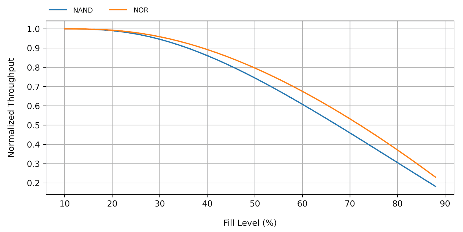
Figure 3 shows \(\eta_\textrm{gc}(l)\) for fill levels ranging from 10% and 90%, for both the NOR and NAND cases. We can now fully appreciate the dramatic impact of garbage collection on write throughput as the fill-level increases.
Discussion
Before discussing the results, let’s first recall the key assumptions that we have made so far to develop our performance model:
- Some kind of flash memory is used, implying the use of copy-on-write and garbage collection (with data consolidation).
- The workload is purely random, that is, write accesses are performed at random, uniformly distributed positions.
- Updates are the size of a page. This requirement though could be relaxed without much impact on the final result, provided that updates remain much smaller than one flash erase block. The case where the update size approaches or exceeds the erase block size is certainly relevant, but must be treated separately (a topic for a future article).
- Implementation-specific limitations (such as metadata update overhead) are purposely ignored, such that our model effectively produces an upper bound on random write performances, regardless of the file system or FTL.
With that in mind, here are our final observations and recommendations:
- Memory space can be traded off for write throughput (and vice versa), so make sure that you use that flexibility to your advantage. At the very least, evaluate the maximum amount of data that will be stored at any given time and make sure that you have realistic performance expectations.
- As a rule of thumb, the fill level should not exceed 80%. Also, the fill-level calculation must only take into account the space available for storing data, which can be less than the entire device. On NAND flash, for instance, some space must be reserved for bad block management.
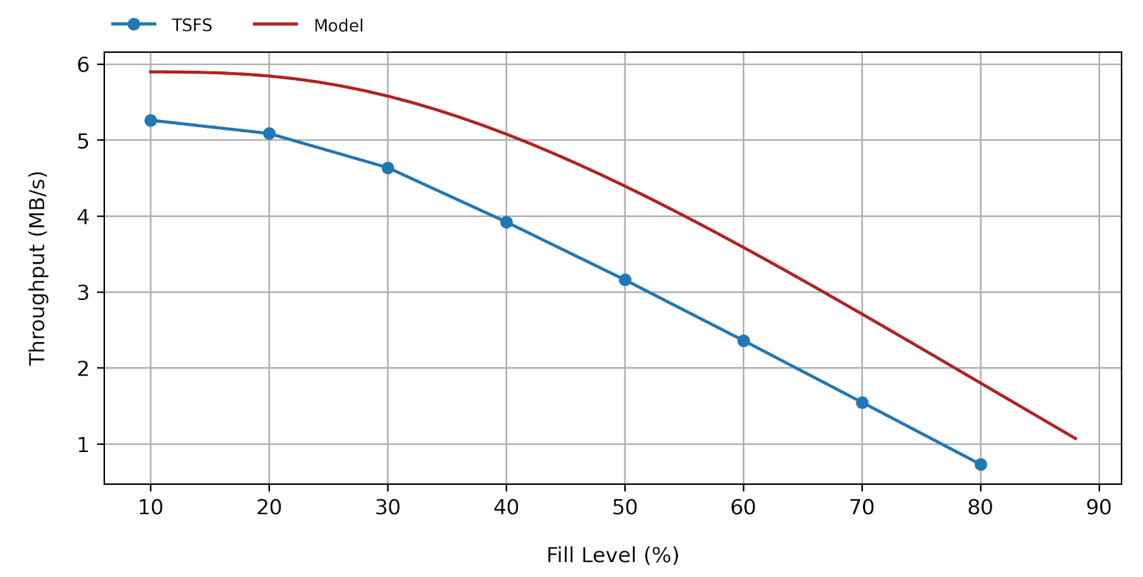
- The actual random write throughput can only be lower than that predicted based on equations 7 or 8. That being said, any decent flash file system should yield performances resembling the model output. For instance, Figure 4 shows how our own flash file system TSFS performs on a QSPI SLC NAND flash with a raw write throughput of 5.9MB/s compared to the corresponding model predicition.
- Predictions based on equations 7 or 8 can help you determine whether your requirements make sense or not. However, it is no replacement for actual measurements, so make sure to include continuous performance testing as part of your application development.
Conclusion
That wraps it up for this article. We do hope that you have learned a thing or two regarding flash storage performance. In future articles, we will cover other important flash performance aspects such as worst-case write latency and other fundamental performance tradeoffs such as that between read and write performances. In the meantime, please feel free to contact us for advice on embedded file systems or any other embedded-related topic.