This is part 1 of a series of articles discussing the configuration of the Xilinx MicroBlaze soft CPU core when targeting an RTOS application. This series will focus on the software aspect of the MicroBlaze configuration. However, before tackling the numerous configuration options available to the MicroBlaze, it is necessary to introduce the various memory hierarchies possible with a MicroBlaze design.
If you are unfamiliar with the MicroBlaze there is a large collection of tutorials and getting started documents on the internet. Of note are Adam Taylor’s MicroZed Chronicles which contain many articles related to the MicroBlaze including a video tutorial on how to get started using the Vivado Design Suite.
MicroBlaze Memory Hierarchy
Owing to the flexible nature of FPGAs, the MicroBlaze can be implemented using many different memory configurations. This includes local tightly coupled memory, block ram from the FPGA fabric as well as various external memory types including DDR SDRAM, SRAM and QSPI NOR flash. Every type of memory, except local memory, can be private to the MicroBlaze or shared with other DMA masters. And in all cases, the implementer can add data and instruction caches. Nearly all of the possibilities can be divided into three categories discussed below, along with a fourth variation related to memory sharing. It’s important to note that these three categories are not exclusive, and it is quite possible to implement all three at the same time in a given system.
Local Memory
The MicroBlaze can use a form of tightly coupled memory with a very low access latency through a dedicated interface, named the Local Memory Bus (LMB). As shown in the following diagram, the MicroBlaze has, at a minimum, three external interfaces. In the diagram, M_AXI_DP is the peripheral data port which the MicroBlaze uses to access the various peripheral registers. The other two, DLMB and ILMB are respectively the local memory buses for data and instruction fetches by the CPU core. It is to those two interfaces that the local memory region is connected.
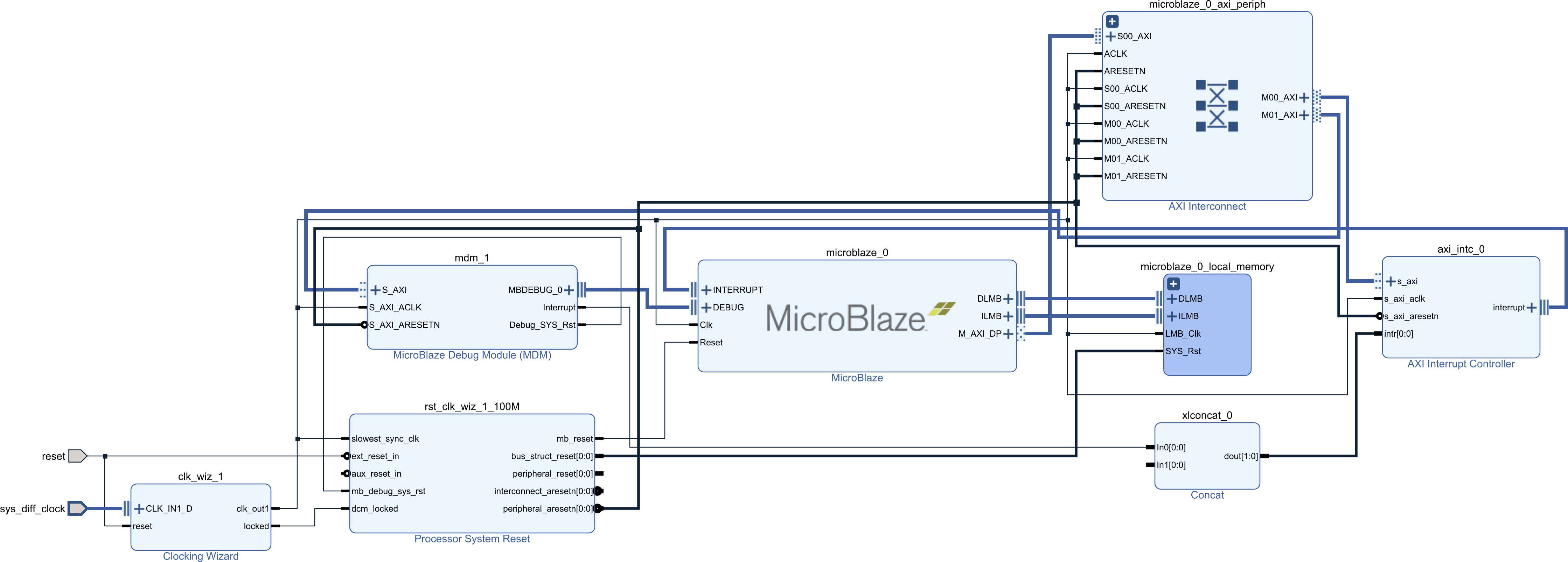
Regardless of the memory configuration, a little amount of local memory is always required for the MicroBlaze boot code. However, if sufficiently large, the program’s instructions and data can be stored entirely in the local memory. Since the LMB has a single cycle access latency, running entirely from local memory negates the need for caches, reducing the resource usage of the MicroBlaze core.
However, the local memory has a few important shortcomings. First it is limited in size, even on a large FPGA, the requirement for single cycle access limits the amount of memory that can be attached to the LMB. Second, the local memory is always private to the MicroBlaze, meaning it cannot be reached by other DMA masters in the system. However, even if external memory is required for any reasons, application developers should remember that the local memory is always available for selected code and data. In any configuration the local memory will function similarly to Tightly Coupled Memory(TCM) found in some SoCs. A previous article, discussing on chip memory, goes into more details of TCM.
AXI Block RAM
If local memory is insufficient, or shared memory is required, block RAM connected through an AXI interface is an option as shown below. You’ll notice that the LMB ram is still there as it’s required, but two new buses connected to an AXI SmartConnect are added to the MicroBlaze. The two new buses are the MicroBlaze data and instruction cache ports. These are then connected to the AXI interconnect which contains a single slave an AXI block ram. It is possible also to connect the block ram through the peripheral AXI interface but this is less efficient.
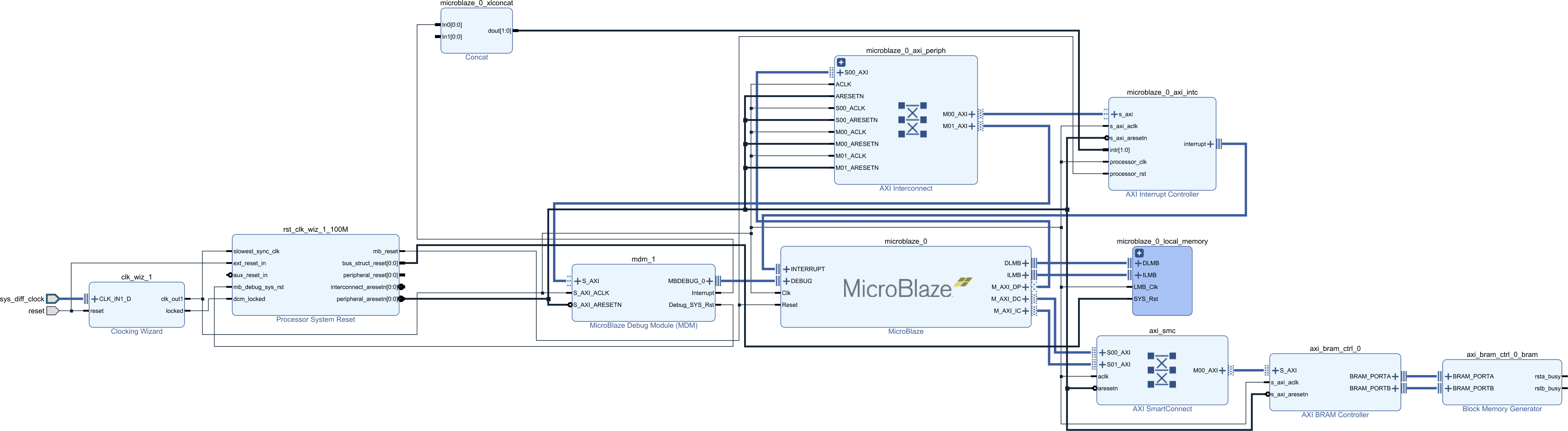
From an FPGA resource perspective, this is very similar to the local memory discussed previously. The difference is that it is accessed by the MicroBlaze through an AXI interface. This allows sharing the memory with other bus masters through an AXI interconnect.
However, the fact that memory accesses must go through an AXI interconnect means that the access latency is higher compared to the LMB. On top of that, shared access brings in the possibility of contention further increasing access latency and decreasing available bandwidth. In this configuration, cache memory may become necessary to maintain the MicroBlaze performance to an acceptable level.
When caches are included, the MicroBlaze will perform any cacheable access through the dedicated AXI interfaces allowing for a bewildering variety of ways to partition the instruction, data and peripheral address space.
External Memory
Finally, if the memory requirements are larger than what can be reasonably implemented within the FPGA there is external memory. External memory is usually either RAM (DDR, SRAM) or some form of non-volatile memory such as QSPI NOR. In the schematic, the MicroBlaze is connected to a DDR interface again through an AXI SmartConnect.
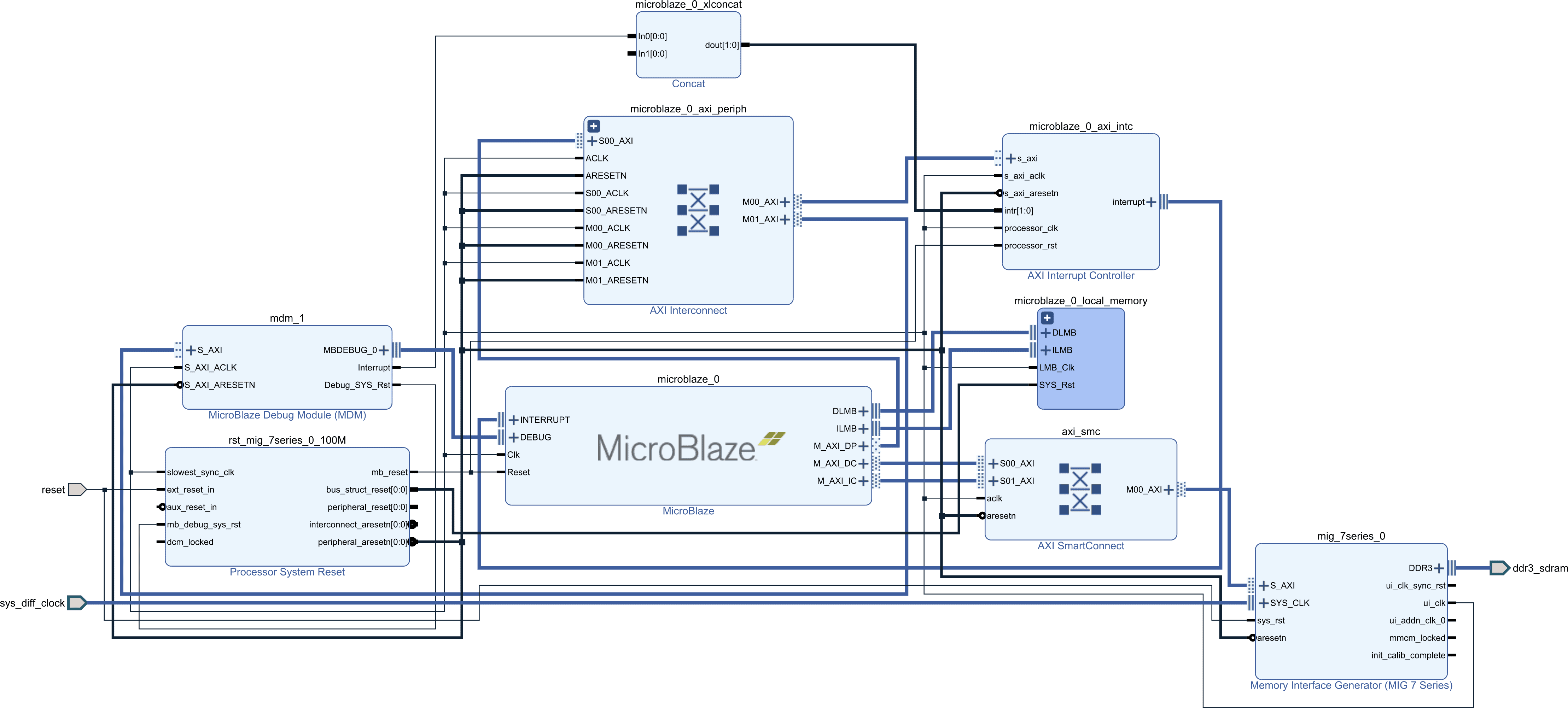
External RAM can contain both code and data while non-volatile memory, usually QSPI NOR, can contain code and read-only data. Note that external QSPI NOR working in XIP (eXecute In Place) mode cannot easily be written. As such, if code is intended to be executed directly from the QSPI NOR another non-volatile storage must be added to the system if a file system is required.
When the MicrBlaze is executing instructions from external memory, be it RAM or ROM, cache is pretty much mandatory to attain any reasonable level of performance. At this point the question is more about optimizing the cache size and configuration to maximize the application performance while reducing the FPGA resource usage.
Shared Memory
With the AXI block RAM or external DDR a common interconnect must be used with other DMA masters, otherwise they won’t be accessible to those masters. For example, in the following diagram an AXI central DMA has access to the same external DDR memory as the MicroBlaze through the use of a common AXI interconnect.
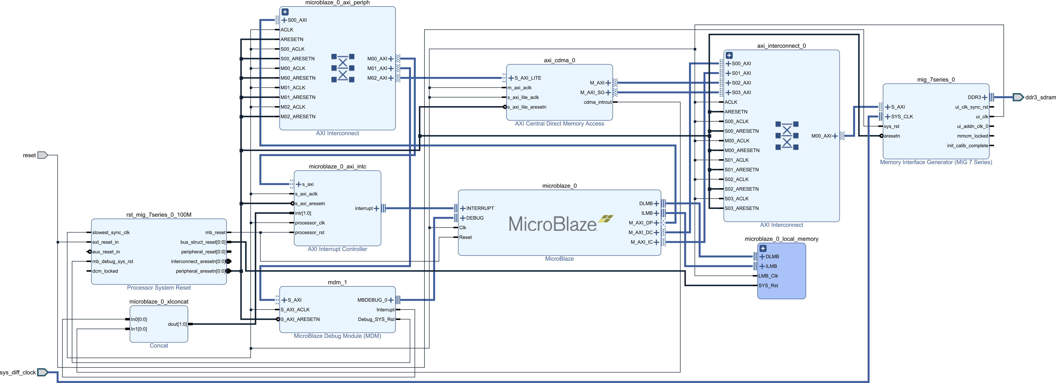
A shared memory region could also be connected to the AXI peripheral data port. In that case the accesses won’t be cached. This means that cache maintenance operations won’t be necessary from the application to ensure coherency of the DMA memory. However, it also means that access to the shared memory won’t have the performance benefit of the data cache.
Conclusion
The hierarchy designs presented in this article aren’t the only options available to the MicoBlaze, but they are the most common. It would be possible to add additional components, such as an L2 cache somewhere in the hierarchy. But at some point the incremental cost of a complex memory hierarchy will outweigh the benefits of using an FPGA. As such, to properly balance the hardware cost and power usage it is important to finely optimize the memory configuration of a MicroBlaze with respect to the application requirements.
Click here to read the second part of this series going over the various configuration parameters of the MicroBlaze.
Questions or comments?
Do not hesitate to contact us at blog@jblopen.com. Your questions, comments and, suggestions are appreciated.