This article is the third and final part (See part 1 and part 2 for the previous articles) of a series of articles discussing the Xilinx MicroBlaze soft CPU core configuration when targeting an RTOS application. This series focuses on the software aspects of the MicroBlaze configuration and the impact of the various MicroBlaze configurations on an embedded application running under an RTOS. This article aims at helping developers and designers who must configure a MicroBlaze system. Especially early on in the development process where the final firmware is not available for benchmarking and tweaking. At these early steps it is often necessary to select a good approximation of the final configuration to have a good idea of the resource usage of the MicroBlaze.
This article will look into details the cache configuration for the MicroBlaze that was skipped in part 2. Configuring the cache correctly is critical to the overall performance of a MicroBlaze system and can also take a considerable amount of FPGA resource, especially block RAM. When configuring the cache, the goal is to use the minimum cache size required to meet the application’s performance but no larger. This is, however, difficult to decide early in the development cycle if the final application isn’t yet available. This article will attempt to give some general guidelines and tips to help system designers to configure the MicroBlaze caches.
The MicroBlaze Caches
The Xilinx MicroBlaze has an optional level 1 instruction and data caches or configurable size and line length. Both caches use direct mapping (a.k.a 1-way associative). The instruction cache can support an optional prefetch stream and both caches attempt to improve interconnect performance by transforming multiple single word accesses into AXI bursts. An additional feature of the data cache is that each word in a cache line has a dirty bit, meaning the cache does not generate line fills on aligned word writes and only writes the necessary data when evicting a cache line.
Although it won’t be discussed in this article there is also a system cache IP available within Vivado that could be used as an external L2 cache for the MicroBlaze.
Why is the Cache Useful?
CPU caches have two main purposes. The first, and most obvious reason, is to reduce the average latency of data and instruction fetches from main memory. In turn, this improves the overall CPU performance by reducing the amount of time the CPU is waiting for data or instructions.
The second purpose is to reduce the bandwidth on the interconnect and main memory. Even if modern DDR3/DDR4 memory has rather incredible bandwidth, it is still fairly limited compared to the rate at which a modern CPU can consume instructions and data. Even more so in multi-core architectures. In all those systems, caches have the effect of reducing the bandwidth requirement. Often time, large L2 or even L3 caches are used to reduce the bandwidth pressure on the memory hierarchy more than trying to improve the CPU instruction and data throughput directly.
In a MicroBlaze system the L1 instruction and data caches are more targeted at improving the CPU performance, but the impact on the main memory bandwidth should not be neglected for systems with many DMA masters competing for memory bandwidth.
Cache Performance Degradation Modes
Cache design and performance analysis is a complex subject and usually beyond the amount of effort that can be expanded into designing a MicroBlaze system. Without going into an in-depth analysis, it is good to keep in mind how a cache can fail to perform as well as would be expected. This can happen mainly in two ways. First it can run out of space. This means that the total local data accessed at high frequency by the application, sometimes called the working set, doesn’t fit into the cache. In this situation useful data is thrown out of the cache too often and too early, before it has a chance of being used again. Application performance can degrade very quickly once the working set grows beyond what can fit into the cache.
The second, and more subtle way, is to run out of space in a set. Without going into details, CPU cache are usually set-associative, meaning that every memory location can only be cached in a few locations into the cache. (Values from 2 to 16 are common). This means that if the working set contains useful data at multiple locations competing for the same cache set, some of the data will get evicted, even if there is free space elsewhere in the cache. Running into a space shortage within a cache set can severely limit an application performance. In the case of the MicroBlaze the cache is direct mapped, meaning that every memory location can only fit in one location into the cache. This makes it prone to the problem described but there is, however, a few ways to mitigate the problem. The first is to increase the size of the cache, which is inefficient, the second is to implement a victim cache which is supported by the MicroBlaze.
Is Caching Required?
There are a few scenarios, explained in the first article where caches are not needed. When instruction and data are completely located in local memory, the cache becomes irrelevant. It’s also possible to have instructions in local memory but data elsewhere, in which case the instruction cache is not needed but the data cache should stay enabled.
Cache Configuration Panel
The cache configuration panel is available in both the configuration wizard and the advanced configuration section. Like the previous article we’ll cover each configuration individually. Note that many options are not available if “Area Optimization” is selected in the general panel.
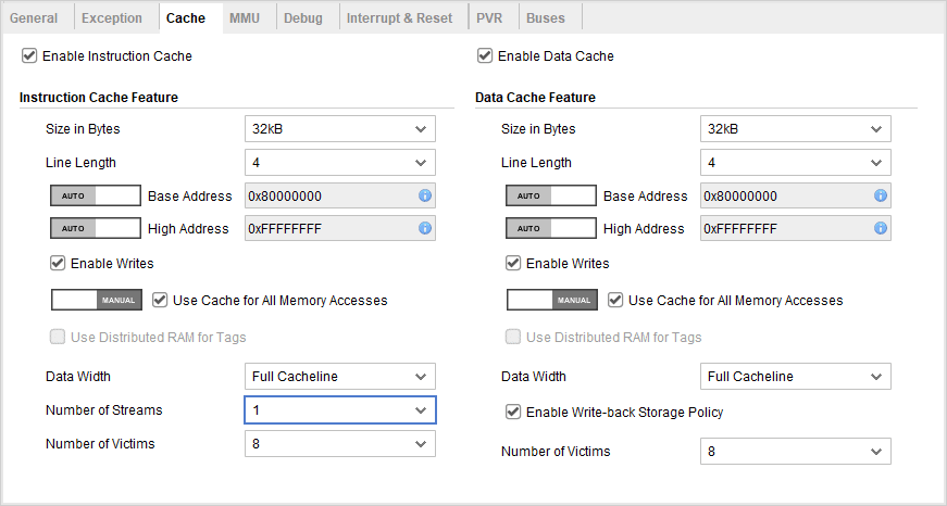
Enable Instruction/Data Cache
The first set of configurations allows to enable the data and instruction caches. It is possible, if desired, to only enable one of the cache if the other isn’t required for the application.
Cache Size in Bytes
The cache size is probably the most difficult option to configure. It’s difficult to predict the required amount of cache to reach a specific level of performance without doing extensive benchmarking. However, a reasonable cache size will usually fall between 4KiB to 32KiB. A cache size under 4 KiB will very likely have performance issues when running from DDR, especially when working with an RTOS. At the other end of the scale, the simplistic nature of the cache and with the clock speed involved it is unlikely that a cache larger than 32KiB will make a significant difference in performance. It is important to note that large caches will occupy a significant FPGA area and likely negatively affect the maximum achievable frequency.
It is also possible to configure different sizes for the instruction and data caches. This should probably be reserved once the application is well developed and careful benchmarking can be performed to tweak the individual cache size. Otherwise, a good starting point would be to keep the two caches of equal sizes.
Line Length
The cache line length, measured in words (4 bytes for 32-bit MicroBlaze) is the size of each cache block. Usually, a larger cache line size has a tendency to improve performance, especially when running from DDR memory. This is especially true on the MicroBlaze since linefills are not performed on write operations. Larger lines also reduce the amount of block ram required to store the tags. Larger line will, however, impact the resource usage of other features such as the victim cache and the data width of the cache ports.
Base Address and High Address
The two address configuration selects the cacheable memory range. The cacheable accesses made within this range will use a dedicated set of AXI ports to access the external memory and should match the location of the intended memory in the interconnect.
Enable Writes
The enable writes options aren’t necessarily the most intuitively named. What they do is enable the WIC and WDC instructions allowing flush and invalidation of individual cache lines. On the data cache side this can be important for DMA drivers who may need to perform cache maintenance operations on shared buffers. On the instruction cache side this is less useful and is usually only used when program instructions are modified or loaded at runtime.
Disabling those two options have a negligible impact on resource usage so they can be left enabled.
Use Cache for All Memory Accesses
These options controls the port used when the caches are disabled. When enabled, the dedicated cache ports will be used for memory access that falls within the cacheable memory range even when the caches are disabled. Otherwise, when a cache is disabled the peripheral AXI ports are used instead. It’s important that this option is configured correctly, otherwise the MicroBlaze might fail to work if the instruction memory isn’t reachable. The default setting of enabled is usually the correct configuration.
Use Distributed RAM for Tags
These options will cause the cache tags to be stored in distributed RAM instead of block RAM. This saves block RAM and can increase the achievable MicroBlaze frequency at the cost of additional FPGA logic. The option to use distributed RAM is only available for smaller caches and is also affected by the line length. Larger cache line length will allow larger cache size to use distributed RAM compared to smaller line length.
These options do not have any concrete software impact and are mostly dictated by system design considerations.
Data Width
The data width controls the external AXI port width used to perform cacheable accesses. Larger width, in theory, allows a cache line fill or write to be done in a single AXI operation instead of a burst access taking multiple bus cycles. Larger width does have a negative impact on resource usage, however.
To be of any use the external memory and interconnect should be of the same size or higher otherwise the advantage will be nulled by the addition of a data width converter in the AXI interconnect.
Number of Streams
This is for the instruction cache only an enables a prefetch buffer allowing the instruction cache to speculatively fetch instructions. Although this somewhat increases resource usage, it is usually recommended to improve the CPU performance.
Enable Write-Back Storage Policy
The write-back option is only available for the data cache since the instruction cache can’t be modified by a CPU write. If disabled, the data cache will function as a write-through cache which means that data writes will be sent to memory immediately. In the case of the MicroBlaze, the write-through cache won’t perform write allocation which means that written data isn’t immediately cached unless they are already in the data cache. With write-back policy the written data is written to the cache and sent to main memory only when evicted from the cache. This improves performance and usually reduces the external memory bandwidth usage.
Some operating systems or drivers may require a write-through cache to reduce the amount of cache maintenance operation required. However, a write-through cache can severely limit the performance of an application since the CPU is affected by the main memory write latency.
Number of Victims
Both the instruction and data caches can have an optional victim cache that can store a limited number of recently evicted cache lines. There is more than one way to look at a victim cache, but for a main cache with limited associativity like the MicroBlaze the victim cache main use is to mitigate the performance issues of the direct mapped cache. For anything but the simplest application the victim cache should probably be enabled at its maximum supported size.
And that’s about it for the cache configuration.
Click here to go back to part 1 of this series discussing the memory hiearchy of the MicroBlaze. Otherwise click here to read our follow-up series on the MicroBlaze performance.
Questions or comments?
Do not hesitate to contact us at blog@jblopen.com. Your questions, comments and, suggestions are appreciated.