On chip ram or internal RAM, often abbreviated OCRAM or OCM has been around since the earliest System on Chips(SoCs). This articles goes over general purpose On-Chip RAM as well as more specialized forms such as Tightly Coupled Memory (TCM) and DMA buffers. We discuss major features and design considerations that could impact an embedded application using OCRAM. The focus is on high performance SoCs and application processors. On chip memory for lower performance MCUs such as Cortex-M has a different role and are usually designed and optimized differently compared to their SoCs counterparts.
In the beginning, on chip memory was relatively small and primarily used by bootloaders or as scratch memory. On-chip RAM has since evolved in terms of size, speed and features as SoCs became more complex to often include error detection and correction, multiple ports and additional security. The wide variety of uses for OCRAM means that there are different design decisions and constraints available to SoC designers, which can have some impacts on the intended usage from the point of view of an application developer.
What is On-Chip RAM?
On chip RAM is one of possibly several types of on chip memory (OCM) available on a SoC. The other types can include Read-Only Memory. For example ROM, Flash, EEPROM and even OTP fuses could be considered a form of data storage available on a SoC.
On chip RAM is, more often than not, implemented as a fast low-latency static RAM. It usually requires little to no configuration before use meaning it can be available early within the boot sequence. As such, it is often an important component of the boot process, providing a small quantity of RAM to the bootloader. This is mostly because the main external SDRAM hasn’t been initialized yet. After booting, it is usually available for use by the operating system and application as required.
OCRAM Features
OCRAM comes in various sizes with different features and characteristics designed to optimize them for a specific SoC’s intended applications. Other than the size, one of the most important characteristics of an on-chip RAM resource is its location within the cache and bus hierarchy which we’ll discuss below.
Size
The primary characteristic of an OCRAM is its size. The amount of available on chip RAM can vary considerably between SoCs, from a few kilobytes to many megabytes. Larger sizes tend to be slower with a higher access latency. The relation between size and speed isn’t exactly linear, however, and varies from SoC to SoC. Finally, sizes from a megabyte and up are usually meant to be used as main memory, possibly replacing external SDRAM. Larger on-chip RAM can also be designed with the assumption that L1 cache is used between the OCRAM and the CPU.
OCRAM Location
OCRAM can be broadly categorized into three types depending on their location with respect to the CPU core.
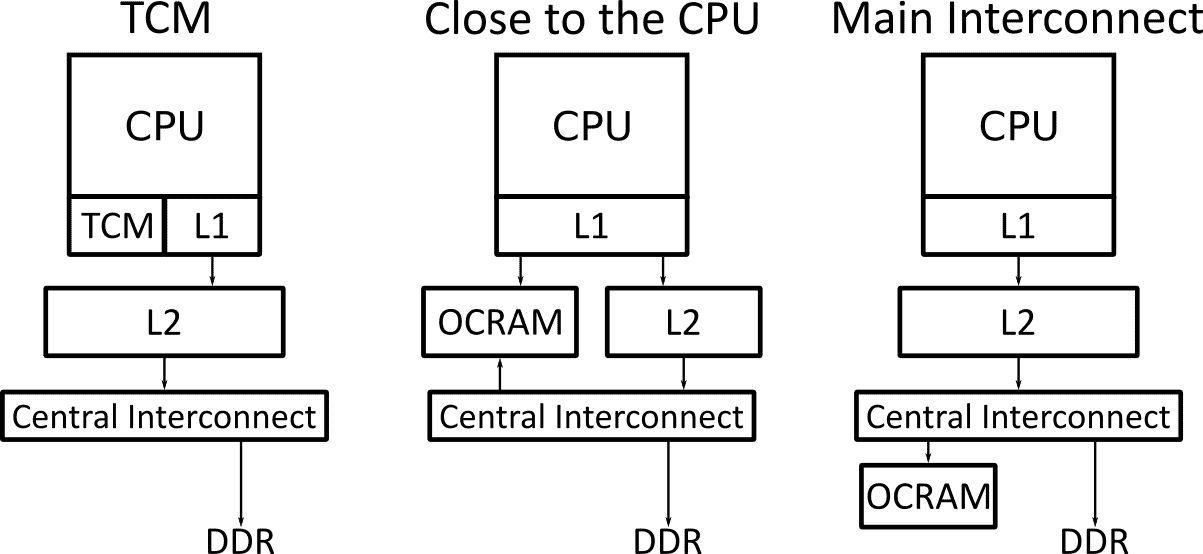
Tightly Coupled Memory (TCM)
While rare in the world of application processors, Tightly Coupled Memory or TCM for short is worth discussing. More common in low power embedded MCU such as the Cortex-M where it’s called Core-Coupled Memory (CCM). TCM can, however, be found in some high performance real time SoCs based on the ARM Cortex-R for example.
Tightly coupled memory is implemented very close to a CPU with access latency and bandwidth at or close to that of L1 cache. This results in very high performance close to the CPU peak memory bandwidth without the use of an intermediate cache memory. This also alleviates the need for cache maintenance operations in some situations. To be effective, TCM must be implemented close to the CPU and clocked at or near the core clock frequency. This means that TCMs are usually kept small, of sizes similar to L1 cache, in order to keep power and die area low.
TCM being connected directly to the CPU core, it is often not accessible by other bus masters such as an Ethernet controller or DMA engine. In addition, in a multi-core system, TCM may not be shareable between cores. When it is available to other masters in a SoC, access from other masters must go through a backdoor port along with some form of arbitration between the backdoor and the CPU owning the TCM region.
Close to the CPU
As a midpoint between a Tightly Coupled Memory and an OCRAM region connected to the central interconnect, on-chip RAM can be connected close to the core through a dedicated low latency port. In this scheme, the OCRAM is often located at a level similar to the L2 cache which offers high bandwidth and low access latency. In a multi-core system this also provides for a fast shareable and possibly coherent memory region accessible from all the cores of an SMP cluster. Access from other masters is done through a second port(sometimes called a backport) along with some form of arbitration scheme between the CPU cores and the other masters.
This type of OCRAM offers a good compromise of features and performance allowing fast low latency access from the CPU without using any central interconnect bandwidth all the while allowing a similarly low latency access from other bus masters. To profit from the close proximity to the CPU, the OCRAM clock frequency must usually be high, increasing the power usage. The high clock frequency and close proximity to the CPU mean this type of OCRAM must be limited to a reasonable size.
Off the Central Interconnect
Finally, the most common location for OCRAM is connected to the central interconnect along with other high-speed peripherals. More rarely OCRAM can be found connected through a subordinate interconnect, but this is rather rare now and is often reserved for special purpose on chip memory.
OCRAM at the main interconnect level are usually clocked at a lower frequency similar to the bus clock, and have a longer access latency. They are also affected by bus contention and access from multiple masters aren’t arbitrated at the RAM level but by the bus between all the bus masters. However, they can be larger, up to multiple megabytes and can be efficiently accessed by peripherals and DMA engines.
Width and Alignment Restrictions
An often overlooked characteristic that must be kept in mind when designing an application relying on OCRAM performance is the width and alignment restrictions. This is especially true if the OCRAM isn’t configured as cacheable. Although most on-chip ram on SoCs that have a CPU core supporting unaligned accessed also supports unaligned access, there may be a considerable penalty associated with an unaligned access. The same can be said for the access width, achieving the performance stated in the manufacturer’s documentation usually requires a specific access pattern.
The effect of width and alignment can be especially important with shared access of the OCRAM between multiple masters for multiple purposes. For example, if the OCRAM is used to store a critical portion of code and data to reduce interrupt latency, a large quantity of unaligned accesses from another CPU or peripheral could significantly increase latency.
The situation with concurrent accesses can be further complicated by the arbitration policy. In some SoCs, the OCRAM will arbitrate between full bus requests while others can break burst accesses in multiple sub-access arbitrated independently.
Error Correction and Checking
OCRAM often support error detection in the form of simple parity and in many cases even support error correction. In either case, the requirement for error checking or correction is application specific, however, it’s important to keep in mind that there may be a specific initialization sequence required for ECC to work properly. Especially if ECC or parity is enabled after the bootloader has run, it might be necessary to either reset or rewrite the entire OCRAM once to initialize the parity bits to a known value.
Dedicated Usage
Some OCRAM regions can be dedicated to a specific use such as a frame buffer for an LCD controller or a private DMA memory region for a USB controller. In that case, it may be possible to use the RAM as general purpose memory if the dedicated function isn’t required. Often this can be done without any configuration or performance penalty. However, sometime a specific configuration step might be required, for example some RAM banks can serve as either L2 cache or general purpose OCRAM which is configurable during the CPU initialization. In other cases, accessing the dedicated memory can be slower when performed from another master.
Security
On top of general access control through the MMU, on chip memory can implement additional access control mechanisms, such as ARM TrustZone. When implemented, the memory is usually called secure memory.
It is interesting to note that even without any additional security features, plain OCRAM can have a few distinct security advantages. First it is usually much more difficult to read or snoop from an external agent than DDR memory. It also doesn’t suffer from persistence issues and is immune to the Row Hammer exploit. Also, with the correct MMU configuration, data stored in OCRAM can be much more resilient to various timing attacks such as Spectre and Meltdown.
Low Power State Retention
The last feature to mention in this article is low power state retention. Especially since most SoCs use external DDR, the internal OCRAM can sometimes be used to store persistent data that is retained even when in a low power state.
That’s about it for now, but further topics on the subject awaits, such as specific configuration issues and information on latency and bandwidth benchmarking.
Questions or comments?
Do not hesitate to contact us at blog@jblopen.com. Your questions, comments and, suggestions are appreciated.