One of our specialties at JBLopen is board bring-up, either for bare metal or various commercial and open source RTOSes. Despite the number of different platforms, CPU architectures and RTOSes out there, low level bring-up, BSP and driver development are rarely discussed in blogs and articles on the web. The same can be said about low-level bare-metal benchmarks which are more representative for evaluating performance of RTOS based applications. While this is hardly my first experience with the NXP i.MX 7, I’ll share in this article some of the important steps we take, writing from scratch, a bare metal environment for the i.MX 7 on the SABRE board. Porting most RTOSes would be similar. This already bulky article focuses on the ARM Cortex-A7 with the Cortex-M4 left for a following article. For reference I’m using DS-5 with ARM Compiler 5 and a Keil ULINKPro D debug probe.
The i.MX 7
Until the availability of the i.MX 8, the i.MX 7 is the flagship of NXP line of heterogeneous multi-core application processors. The i.MX 7 can be seen as the AMP version of the i.MX 6UltraLite with the addition of a Cortex-M4 and a faster core speed. It trades the Cortex-A9 of earlier 6 series for the more efficient Cortex-A7, coupled with the Cortex-M4 in a very similar configuration to the I.MX 6SoloX.
Under the hood, other than the change of CPU core, the i.MX 7 has a few welcome improvements over the A9 based SoloX and others. The Cortex-A core itself supports a faster clock speed of 1.2Ghz over 1Ghz, as well as double the amount L2 cache. Moreover, the A7’s integrated L2 cache is faster and has a lower access latency compared to the external l2c310 L2 cache of the A9. The DDR controller was replaced with a simpler to configure IP which supports up to DDR3-1066 compared to DDR3-800 for the SoloX. The on-chip ram is also doubled in size to 256 kiB.
Another improvement, probably invisible to a lot of developers, is the flatter, more straightforward and versatile clock tree of the i.MX 7. Coupled with a different Clock Control Module(CCM) interface, the i.MX 7 makes it easier to control the peripheral clocks, with fewer interdependencies. This greatly simplifies peripheral partitioning where the Cortex-M4 can change peripherals clock without interference from the application processor.
Hardware setup
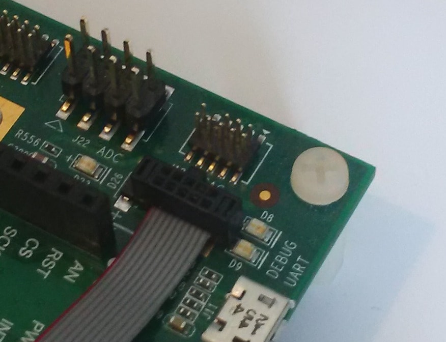
First thing of note is the debug connector. Leaving behind the bulky 20 pins JTAG, the i.MX 7 Sabre board uses the small coresight 10 connector. Per the ARM specification, pin 7 is supposed to be keyed, meaning it should not be present on the male side of the connector. This is not the case on the Sabre board, which requires cutting pin 7 if the JTAG connector is keyed, as can be seen in the picture.
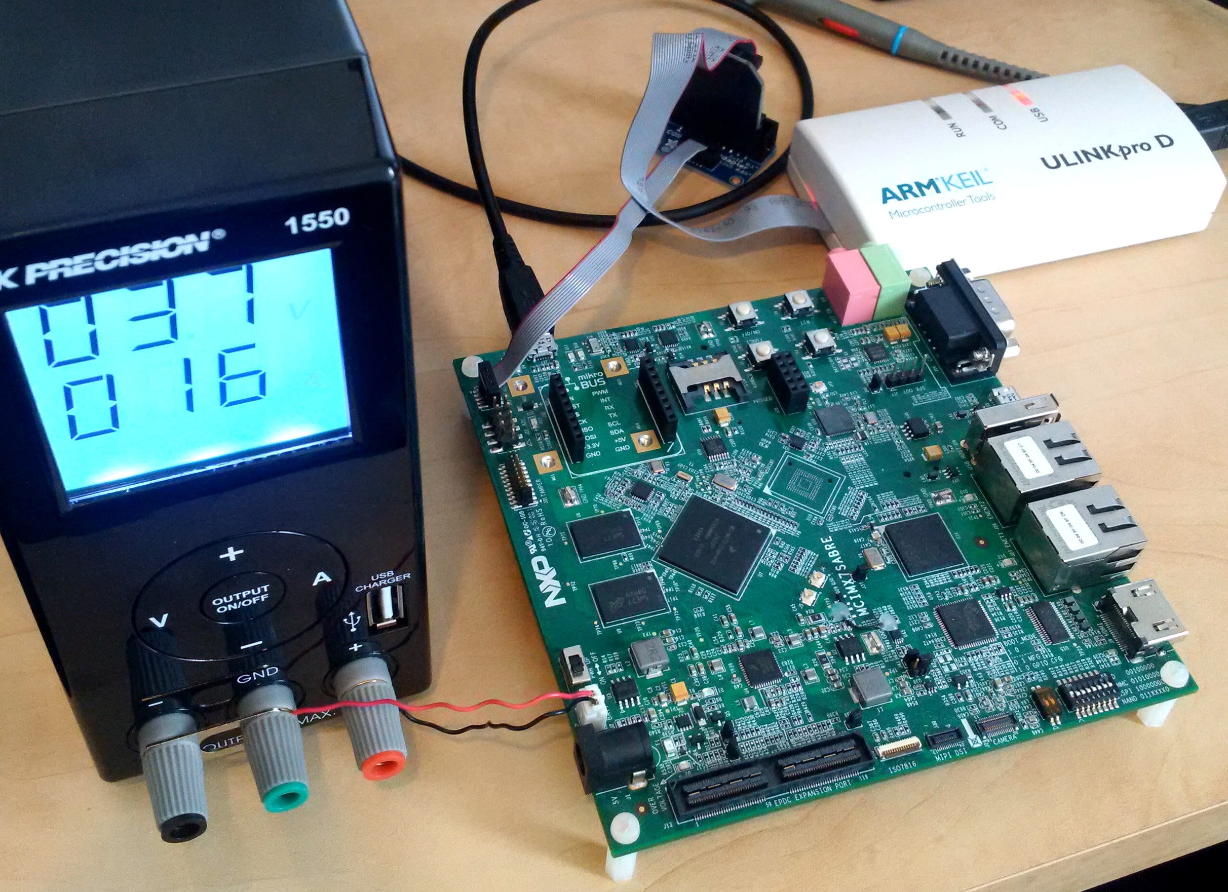
Power is provided either by a 5V wall adapter, with the usual connector or a battery input. I’m using the battery input as we’ll need to do some power measurement, which will also be the topic of a later article. The schematic mentions a nominal voltage of 3.7V for the battery input, looking at the PF3000 PMIC datasheet 3.6V seems to be the absolute minimum to guarantee reliable operations. While the Sabre board isn’t really optimized for low power operations, when using the battery input most of the heavy external components are left unpowered. Also, the input regulator and LED is bypassed, yielding a more representative measurement of overall systems power usage.
Finally, for serial input output, the Sabre has the nice feature of including not one, but two UART to USB converters on one OTG connector. This is very useful when debugging both the A7 and M4 at the same time.
Debugger configuration
Opening a debug connection from DS-5 is quite straightforward, with the choice of connecting to each A7 core independently or debugging both at the same time in an SMP configuration. Even for an AMP setup, I usually prefer an SMP connection when debugging both A7 core since it’s easier to debug.
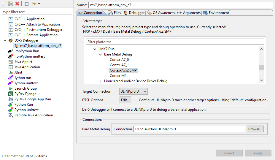
I used the U-Boot code for the mx7 sabre as a base to write a debugger init script (.ds). A ds script is also included with the DDR Stress Test tool from NXP.
MMU Translation table
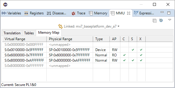
Translation tables for RTOS and bare-metal applications are simple. While it is possible to create a fine-grained page table, it would require two levels of tables, which consumes more space and is slower for the CPU to browse. This leaves 1MiB and 16MiB section and supersections. To improve performance, and reduce latency I prefer to use supersections. With one exception, it’s useful to have address 0x00000000 mapped as a fault. Otherwise, dereferencing a NULL pointer will, in the case of the i.MX7, generate a read or write in the Boot ROM area, making it harder to debug null pointers. On other ARM SoCs with nothing at address 0, you either get a slave error or worst, a hung AXI bus. Since I don’t need anything from the first MiB of address space, I’ll use a 1MiB section mapped as a fault followed by 15 sections of device memory. The rest is straightforward, with everything else using supersections of device memory, the flash memory as normal read-only memory and RAM as normal memory.
Thanks to DS-5’s MMU view feature, confirming correct MMU configuration is the easiest thing.
System timer and RTC check
This whole paragraph should be in bold. It’s surprising how much trouble incorrect frequencies can cause, so very early in the development cycle every embedded developer should check that core timer frequencies are correct. There are a few ways to check the frequency of an internal timer, for example comparing them to the RTC. However, nothing beats the low-tech method of switching a GPIO and measuring with a scope.
I usually like to measure these three items independently; other clocks and timers can be compared to the system timer if necessary.
- System timer frequency
- RTC frequency
- CPU core clock
In all cases the frequencies should be within their source’s tolerance. On ARM processors, measuring the core CPU clock frequency can be achieved using the cycle counter of the performance monitoring unit (PMU).
Having confirmed that we can measure time correctly, it’s now time for some benchmarking.
A7 benchmark
Benchmarking the CPU is useful to verify that performances are what’s expected. An easy benchmark that has very few dependencies is CoreMark, it can be downloaded freely from the EEMBC website. After running the benchmark, the result can be compared with published results.
Running the core at 996Mhz, with CoreMark built using ARM Compiler 5.06 at maximum optimization, the A7 yields 3138 CoreMarks, or 3.15 CoreMarks per MHz. This is a single core benchmark, but if we allow ourselves to extrapolate to two cores, this would mean over 6000 CoreMarks for a low-power application processor. Nor bad at all.
What’s next
An important aspect, power, hasn’t been discussed in this article. At the very least one would have to verify that power consumption is within acceptable limits. More details on power management for the i.MX 7 will be the topic of a follow-up article. Also, stay tuned for the M4 bring-up and benchmarks.
Click here to read the next article on the Cortex-M4 bring-up and benchmarks.
Questions or comments?
Do not hesitate to contact us at blog@jblopen.com. Your questions, comments and, suggestions are appreciated.