Following up on the last piece about the NXP i.MX 7, this article looks at the ARM Cortex-M4 companion of the Cortex-A7 present in the i.MX 7. Or to put it another way, a Kinetis-on-chip since it’s very similar to a high-end Cortex-M4 based Kinetis. This article summarizes my experience writing a brand new bare metal bring up for the i.MX 7. I’ll conclude with some CoreMark benchmarks.
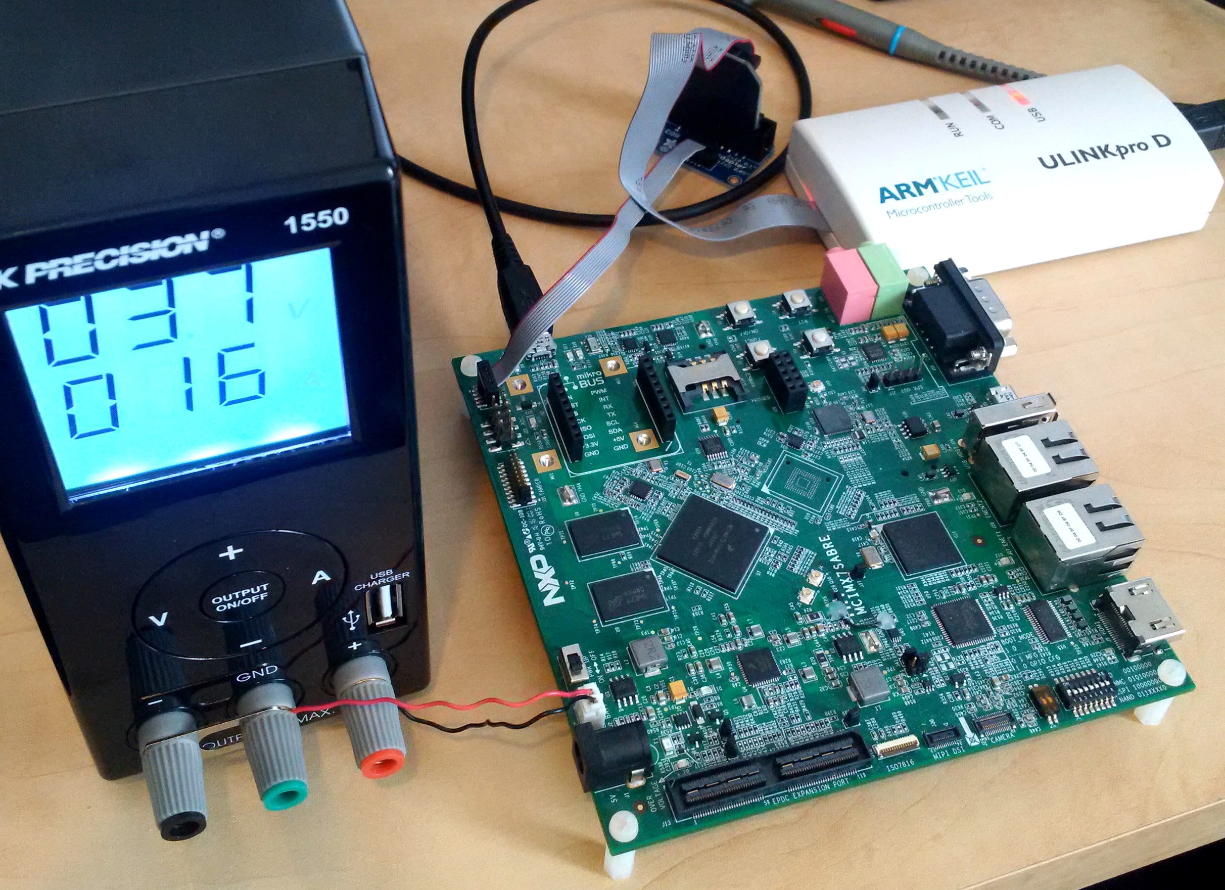
I’m still using the same setup with DS-5 and a Keil ULINKpro D debug probe, same as the previous article.
Booting the M4 is relatively simple, since the A7 takes care of most of the SoC configuration such as clocks and muxes. Debug configuration is also very easy, as again, most of the complicated setup is already done. The most complicated part of the companion M4 is the memory layout. So, let’s jump right into it.
Memory layout
The M4 has a generous selection of on and off chip memories to choose from to store code and data. That includes 64KiB of tightly coupled memory, up to 288KiB of on chip ram as well as external memories such as DDR RAM and QSPI flash. When considering an application memory layout, two important aspects needs to be taken into consideration. First, the M4 uses a modified Harvard architecture with multiple buses each reserved for specific addresses ranges. Second, the included cache controllers are only capable of caching accesses to a specific range of addresses. An incorrect application layout could result in a considerable performance penalty.
System and code buses
All Cortex-M3, M4 and M7 have a separate code and system bus, as well as a private peripheral bus to access the core level peripherals. The code bus is optimized for instruction access, while the system bus is optimized for data access. In the case of the i.MX 7, the code bus can perform instruction and data accesses without any performance penalty. However, instruction accesses on the system bus have an additional cycle of access latency. These kinds of limitations are relatively transparent on most Cortex-M MCU, the on-board flash is connected to the code bus while the on-chip ram use the system bus. On the I.MX 7, however, there are multiple RAM and ROM regions along with aliases of those same regions on both buses. I’ll explain in more details the various choices of application layout along with supporting benchmarks a little later in this article.
For reference, the range for the various buses is the same for all Cortex-M4 which are usually referred to as the ICode (Code bus), DCode (System bus), and PPB (Private bus) in the ARM reference manual.
The ranges are as follow:
Code Bus: 0x00000000 – 0x1FFFFFFF
System Bus: 0x20000000 – 0xDFFFFFFF
Private Bus: 0xE0000000+
Caches
The tightly coupled memories (TCML & TCMU) are designed for the Cortex-M4 pipelined memory access, meaning they can provide instructions and data to the M4 core at clock speed without wait states. Except for those, every other memory, even the on-chip ram (OCRAM) have a much higher latency. To alleviate this, two 16 KiB caches are included on each of the code and system bus. This is very similar, for example, to the K70 cache controllers.
According to the documentation only the following address ranges are implemented in the cache controllers:
DDRC: 0x80000000 – 0x801FFFFF (2MiB)
QSPI: 0x60000000 – 0x601FFFFF & 0x60200000 – 0x603FFFFF (2MiB each)
OCRAM: 0x20200000 – 0x203FFFFF (Entire OCRAM including EPDC and PXP RAM)
From this a few things should be noted. First, obviously, the TCM are not included since they do not need caching. The second is that nothing on the code side is cacheable, meaning the instruction cache is unused on the M4 core of the i.MX 7. I’ll elaborate on this a little later as well.
Putting it all together
Here are the various places where the M4 could typically use for code and data.
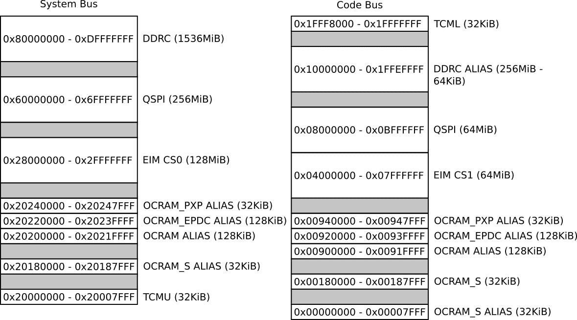
Technically, yes, it would be possible to execute code from storage mapped to the PCIe or programmed in the on-chip ROM but those would be unlikely, so I left them out of the memory map.
While there is a multitude of variations on where code and data are located there are basically two important configurations with a variation where the code is in the QSPI NOR instead.
In all cases, and this is important to remember the initial vector table location is at address 0, always. Which in the case of the i.MX 7 is at the start of the OCRAM_S alias region, so for the A7 to boot the M4 the start address and initial stack must be written to the OCRAM_S region at address 0x00180000. This is an important difference compared to the i.MX 6SX where the initial vector location was in TCM. If interrupt latency is important, it may be a good idea to switch the vector location at runtime to the TCM.
Code and data in TCM
Pretty much the default option, application code goes in TCML and data in TCMU. For reference, here’s a scatter file for that configuration. If, instead, the app code is in QSPI then both TCML and TCMU can be used for data.
TCMU 0x20000000 0x7FFF
{
 APP_DATA +0
 {
 * (+RW,+ZI)
 }

 EXEC_2 +0 UNINIT
 {
 *(PLATFORM_STACK)
 *(PLATFORM_HEAP)
 }
}

TCML 0x1FFF8000 0x7FFF
{
 APP_CODE +0
 {
 entry.o(.emb_text +FIRST)
 * (+RO)
 }
}

OCRAM_S 0x20180000 0x8000
{
 M4_VECTOR +0
 {
 vector.o(PLATFORM_VECTOR)
 }
}
Code and data in DDR
Due to the particularities about the instruction cache, only the data side DDR should be used for code and data. In that case both the TCML and TCMU could be used as fast scratch ram.
DDRC 0x80000000 0x200000
{
 APP_CODE +0
 {
 entry.o(.emb_text +FIRST)
 * (+RO)
 }

 APP_DATA +0
 {
 * (+RW,+ZI)
 }

 EXEC_2 +0 UNINIT
 {
 *(PLATFORM_STACK)
 *(PLATFORM_HEAP)
 }
}

OCRAM_S 0x20180000 0x8000
{
 M4_VECTOR +0
 {
 vector.o(PLATFORM_VECTOR)
 }
}
An important note on using the OCRAM and TCM
In all cases the OCRAM can be used for code and data as it’s cacheable (Not the OCRAM_S however). Same thing goes for the TCM. You may have noticed that I have those always as two separate regions in the scatter file. It’s because they are not contiguous regions of memory, and must not be presented as such to the linker. Everything could appear to work fine, but an unaligned memory access, which is legal on the V7-M architecture, will give erroneous results. Another option would be to disable unaligned access in the compiler but I rather stay on the safe side and not have any objects cross the boundaries between the various ram region. Same thing goes for the cacheable to non-cacheable regions of the DDR, this could generate a mismatched access which has unpredictable results.
Benchmarks
The best way to confirm the entire memory layout, cache and, MPU configurations are correct is to benchmark the core. Theses results are obtained by running the M4 at 270 MHz with maximum optimizations in ARMCC5.
Here are a few results from optimal configurations:
| Configuration | CoreMark | CoreMark/MHz |
|---|---|---|
| TCMU Data & TCML Code | 768.69 | 2.85 |
| DDR Code and Data | 531.73 | 1.97 |
| OCRAM Code and Data | 531.73 | 1.97 |
As expected the TCM yields the best results at 768 CoreMark or 2.85 CoreMark/MHz. The results from DDR and OCRAM show the effect of accessing instructions from the data side of the memory map. Consequently, performance drops to 1.97 CoreMark/MHz.
Now, let’s say we were using a less optimal configuration, or a mis-configured cache. Here are a few results for the curious in various non-optimal scenarios.
| Configuration | CoreMark | CoreMark/MHz |
|---|---|---|
| TCMU Code& TCML Data | 552.74 | 2.05 |
| DDR Code and Data without cache | 24.45 | 0.09 |
| DDR Data and DDR Low Code | 29.6 | 0.11 |
| OCRAM without cache | 56.94 | 0.21 |
All in all, the companion M4 of the i.MX 7 is quite powerful assuming it’s configured correctly. This isn’t the last article planned for the i.MX7, hopefully I’ll have some interesting insight to share about the advanced power management features of the i.MX 7.
Questions or comments?
Do not hesitate to contact us at blog@jblopen.com. Your questions, comments and, suggestions are appreciated.