The concept of the Quad Serial Peripheral Interface, i.e. QUAD SPI or QSPI for short, appears rather simple. Extend the common SPI protocol to use 4 data lanes, thus increasing the overall bandwidth. In practice, however, the answer isn’t as simple. Including the obligatory single, dual and quad data lane modes there are over a dozen variations of the base protocol. As is the form for storage devices, not all variations are supported by every device family. And to make things even more complicated, QSPI controllers often do not support all the variations.
But fear not, in this third entry on the ins and outs of QSPI NOR Flash devices, we look at the Quad Serial Peripheral Interface protocol and its variations in depth. In previous articles, we looked at the hardware characteristics of QSPI NOR devices and the internal memory organization of the flash memory.
This series isn’t meant to be an introduction to NOR flash technology but is more about what differentiates one QSPI NOR flash device from another. And as is usual with our articles, this series puts special emphasis on the impact of device features and characteristics on the software and application design.
The QSPI Protocol
Over the course of this article, we’ll go through most variations of the protocol used by QSPI NOR Flash devices. We’ll start simple, with the basic SPI protocol then move through the variations to reach some of the more complicated QIO, QPI and DDR variations. One thing to keep in mind is that QSPI NOR devices are optimized for read performance. Indeed, QSPI NOR Flash boasts one of the fastest random access performances of all discrete flash storage media, and excellent sequential read performance reaching close to 100 MiB/s sustained bandwidth. Consequentially the various read commands are more representative of the protocol variations than any other command class. As such, we’ll concentrate on the read command protocol while a deeper insight into the command set of QSPI NOR will be left to a future article.
Standard SPI (1-1-1)
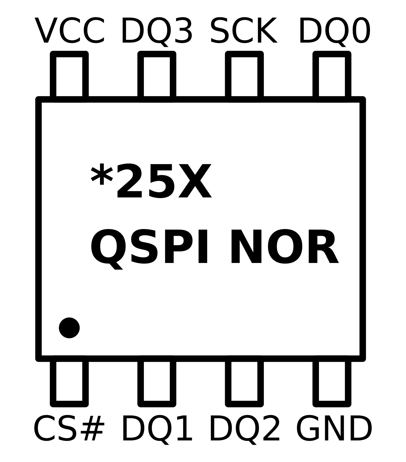
The standard SPI mode is known by many names by the various manufacturers: Standard SPI, legacy SPI, single SPI, single lane, single bit and finally extended SPI. Regardless of which name is chosen by the datasheet they refer to the same thing, the well-known 4-wire SPI protocol. The next figure shows a common pin assignment of an 8-pin device when using the standard SPI mode.
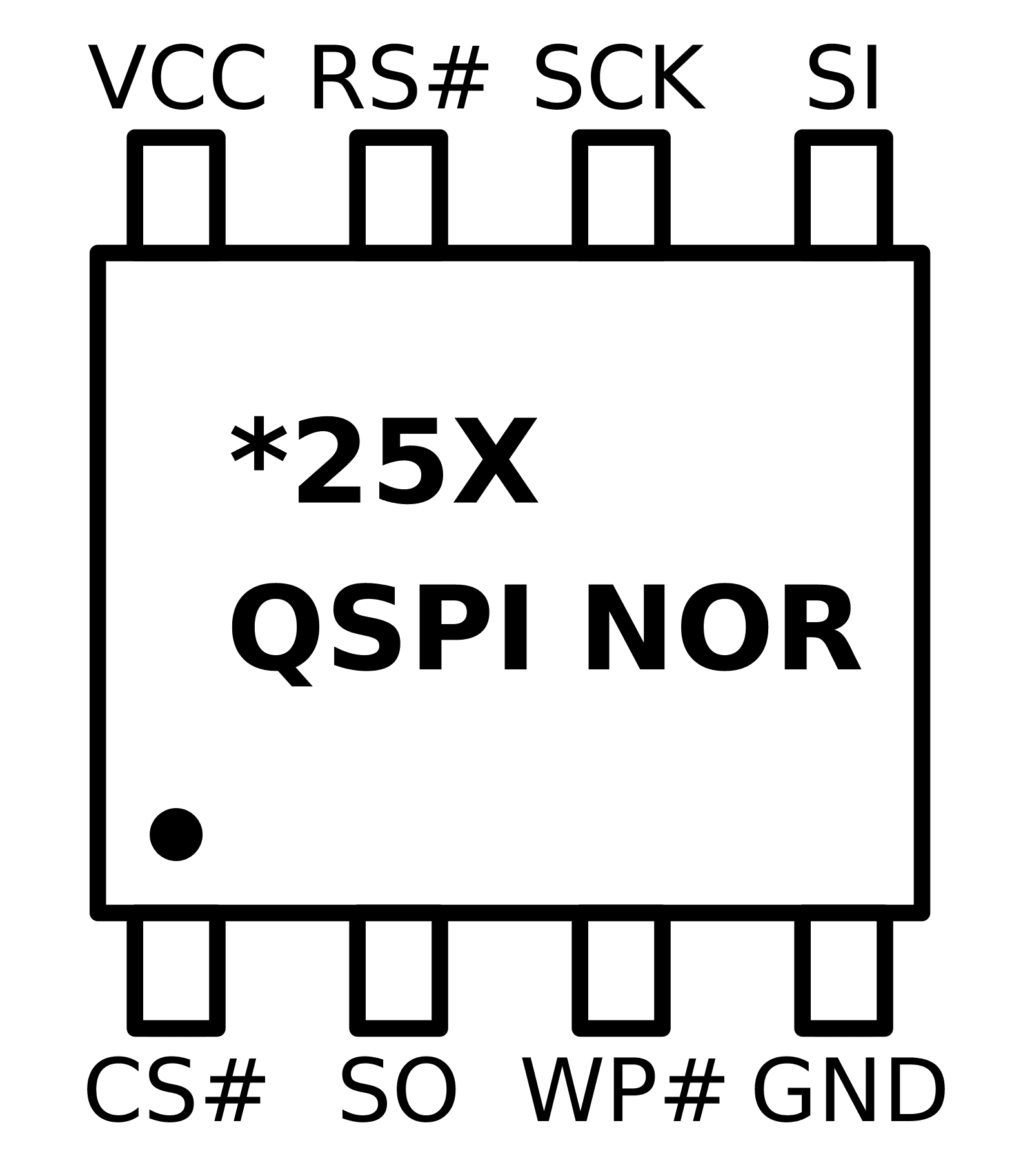
VCC and VSS Supply pins.
Hold/Reset* This pin is either the Hold or Reset signal. Many manufacturers offer both options using either a different part number or a configurable register allowing the pin function to be changed by the host. When configured to be the Reset signal, it simply resets the device when the signal goes low. When using the Hold function the SPI transfer is paused .i.e. held, while the signal is kept low. This allows the host to temporarily raise the chip select line and select another slave device, returning to the paused transfer later.
Write Protect* When the WP pin is driven low writing to the device’s status register is inhibited. This is used to prevent accidentally overwriting the block protection configuration. Note that this is mostly for backward compatibility with legacy applications. Most manufacturers implement an advanced block protection in addition to the legacy block protection. Often when using more advanced block protection features the state of the WP pin is irrelevant.
Chip Select Chip select signal used by the host to start and end a transfer.
Clock Serial clock, data is sampled on the rising edge and shifted out on the falling edge in standard SPI mode.
Slave In Serial data input pin for command, address and data from the host SoC.
Slave Out Serial data output pin for the data read from the device.
Note that signals marked with an asterisks (*) are not available when running in quad mode as we’ll see later.
The following figure shows a basic operation where the host is reading one byte from the NOR flash using the standard SPI protocol.
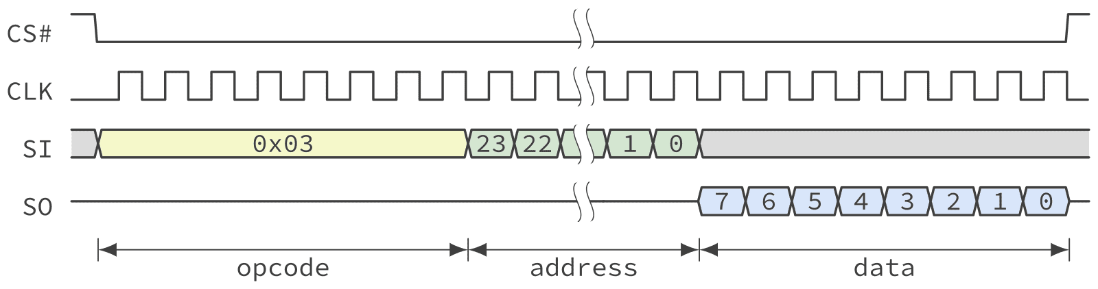
All commands are initiated from the host by toggling the chip select line from high to low. Following this, the host sends an 8-bit opcode with the most significant bit of the opcode sampled by the chip on the first rising edge of the clock signal. In this example the READ command with opcode 0x03 is used. Then the host sends, MSB first, the 24-bit address of the first byte to be read from the Flash. Finally, following the last bit of the address the device shift out the first byte read, MSB first. In this example the read operation is stopped after reading one byte by raising the chip select line. However, it would be possible for the host to continue reading data by keeping the chip select asserted and the clock toggling. The device will, by default, automatically increment the address to be read shifting out subsequent bytes of data.
About the SPI Mode
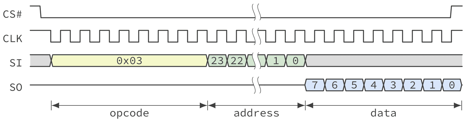
The example shown above uses a clock polarity that is idle low, meaning that the first transition of the clock signal after the chip select is asserted is a rising edge. In the same example, data is sampled on each rising edge. This is often known as mode (0, 0) in SPI bus parlance. Usually, the SPI bus supports 4 different combinations of clock polarity and phase. However, for simplicity and compatibility, QSPI NOR devices only support modes (0, 0) and (1, 1) which are equivalent from the device perspective. In both cases data bits are sampled at each rising edge. The only difference is that in mode (1, 1) the clock is high when inactive, which means that the first clock transition is a falling edge. This effectively adds a half-cycle delay to every operation.
Figure 3 shows the same read transaction as Figure 1 but using mode (1, 1). Note the extra delay before the opcode is shifted in.
About the Address Length
The original QSPI protocol uses 3 bytes for the address which limits the addressable memory to 16 MiB (128Mbit). However, larger devices must support 4-byte addresses which can be achieved in different ways. The easiest way is through a dedicated 4-byte address command set which expects 32-bit addresses. A second method is through a configuration register or a dedicated command that can be used to modify all legacy commands to accept 4-byte addresses. Finally, many QSPI NOR Flash implements an extended address register where the upper byte of the address can be set acting as a sort of bank selection register.
One thing to keep in mind is that not every QSPI controller support 4-byte addressing. This should be checked before using a QSPI NOR device over 128 Mbit.
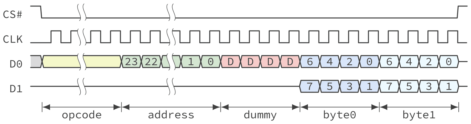
Fast Read (1-1-1)
The SPI protocol is solely driven by the master and is also synchronous, meaning that when reading from the NOR chip the device must be ready to provide the first byte of data as soon as the address is transferred. From the example in Figure 2 one can notice that the address is shifted most significant byte first, this gives the device a bit of extra time to prepare the read data since it can start accessing the correct page before the last byte is transferred. This works well for low to medium bus clock speed.
However, as the SPI clock frequency is increased there is a point where the device can’t get the first byte of data fast enough. This frequency is usually between 50 and 80 MHz and is quoted within a device’s datasheet AC characteristics section as the maximum frequency for the normal read command (opcode 0x3). Over that frequency another read command must be used, called fast read. Figure 4 shows an example of reading one byte using the fast read command.
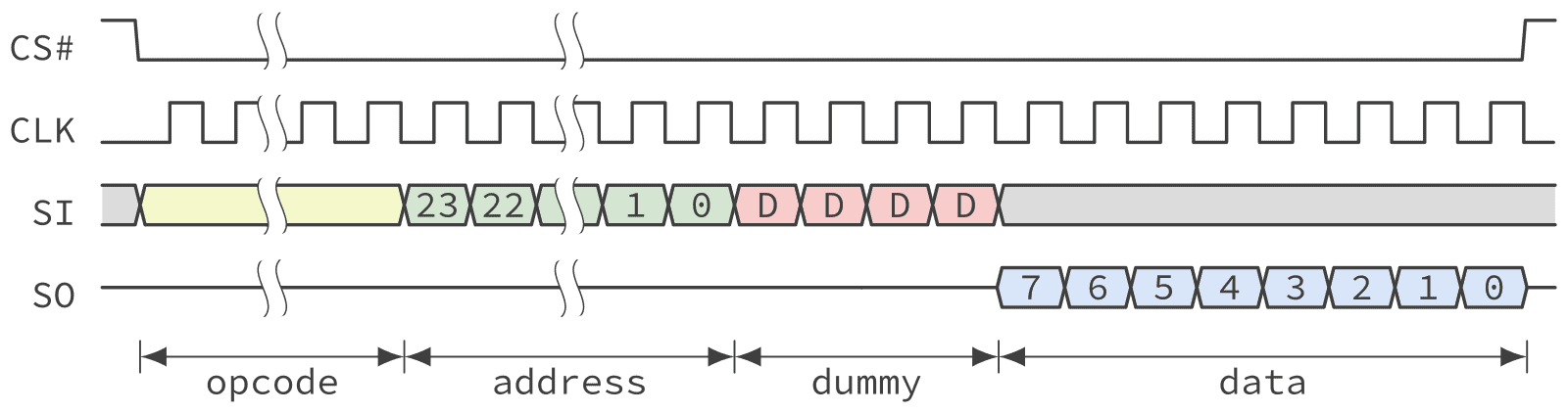
As can be seen from Figure 4, a sequence of one or more dummy cycles is inserted between the end of the addressing phase and the moment the device start shifting out the first byte of data. This gives the device extra time to access the Flash memory. Dummy cycles are also referred to as dummy bits by some manufacturer. Also some QSPI controller are unable to transfer an odd number of dummy cycles, meaning that dummy bits must be sent in multiple of 8 in which case they are often referred to as dummy bytes in those controller’s documentation. In all cases the number of dummy cycles to be used must be agreed upon between the host and NOR flash device. This is usually accomplished by setting a configuration register with the number of cycles to use for the fast read command.
We’ll look into the aspects of selecting and configuring the number of dummy cycles in the next article where we’ll look at the command set and configuration registers of QSPI NOR devices.
A Word on the Value of Dummy Cycles.
In QSPI timing diagrams dummy cycles are sometimes shown as High-Z or not-care/Unknown. This is not always the case, however. For some devices, the value of the dummy bits may have a significance. Especially the first bit can be used to stay in or transition from/to an optimized read mode. Some devices may also transmit a data learning pattern in the last few dummy cycles which can be used by high-performance controllers to measure the phase shift between the clock signal and the returned data.
Dual and Quad SPI
QSPI NOR devices never send and receive data at the same time. Which means that with the normal pin assignment of the SPI bus only one of the data pins is used at any one time. In other words, the bus is underutilized. The usable bandwidth can be doubled by using both pins at the same time. This is the idea behind Dual SPI. And while we’re at it, why not double the number of data lanes to 4 further doubling the bandwidth and we now have the well known Quad SPI protocol. Dual and Quad SPI are also referred to as Dual Output and Quad Output modes in some datasheets.
Obviously to use Dual and Quad SPI the pin assignment must be changed as shown in Figure 5.
As can be seen from the diagram when using Dual SPI, the slave in and slave out pins become bidirectional data pins D0 and D1. Furthermore, for QUAD SPI operation the write protect and reset/hold pins become D2 and D3. Obviously while in QSPI mode the functionality offered by the WP and RESET/HOLD pins cannot be used. It is important to note that those pins will perform there original function before switching to QSPI mode. Especially for the RESET pin it’s important that it is not inadvertently driven low prior to entering QSPI mode. In some designs an external pull-up might be required. Alternatively, most QSPI Flash devices offer the possibility to disable those pins at start-up with the use of a non-volatile configuration register.
Dual SPI (1-1-2)
By using both data lines in a bi-directional fashion a QSPI NOR running in dual SPI mode can double the read bandwidth without using additional pins. The protocol of dual SPI operation is shown in Figure 6.
In dual SPI mode, selected by sending a specific opcode, the command and address are still sent using a single data line D0. However, the returned data are sent using the two data lines thus being able to transfer a byte every 4 cycles instead of 8.
Quad SPI (1-1-4)
Why stop at two lines if you can have four. By extending the concept of dual SPI with the addition of two more data lines, we get the QSPI protocol. Again, this is selected using a specific opcode when performing the read operation, signalling the NOR Flash that data should be returned on 4 lanes as shown in Figure 7.
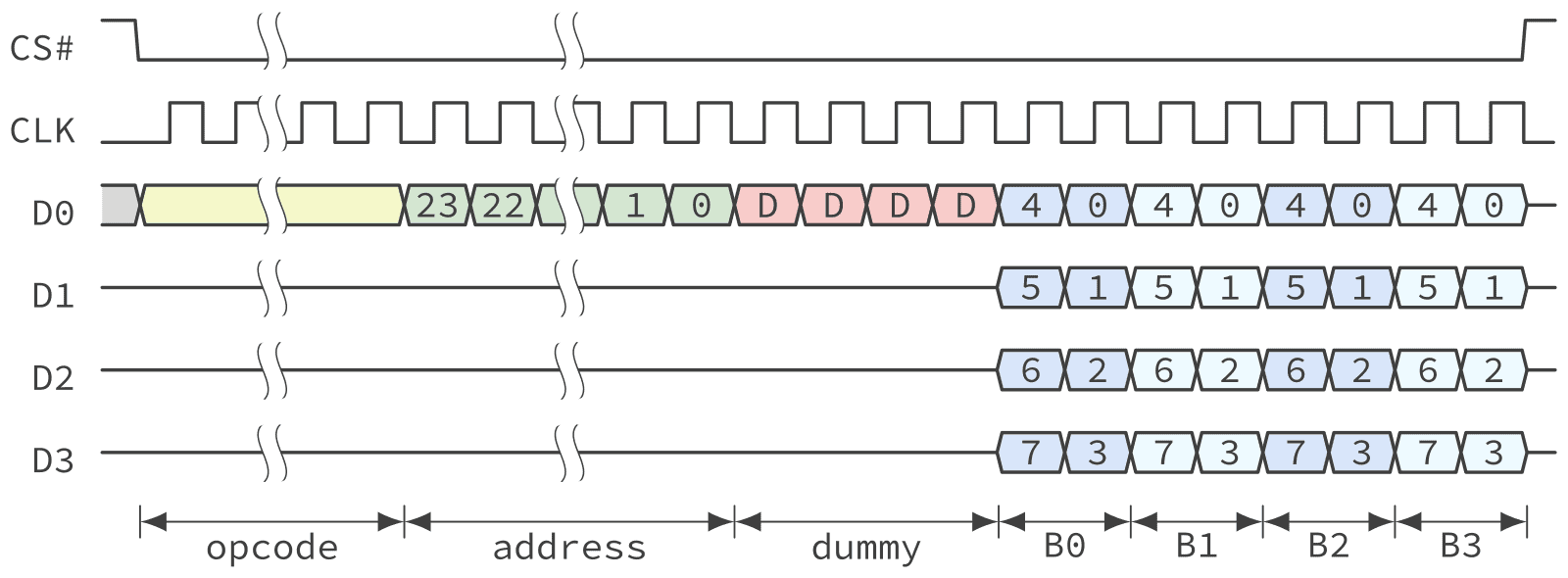
By using 4 data lanes, a byte can be read every 2 cycles thus quadrupling the bandwidth of the standard SPI mode.
The Story so Far
The previous sections presented the basic modes that can be used to read data from a QSPI NOR Flash. Those modes are supported by all QSPI devices. Also, nearly all QSPI controller can use those modes across the various manufacturers and part families of QSPI Flash devices.
However, there are many more protocol variations aiming at improving the I/O performance of QSPI Flash devices. These variations, however, are less standardized between device families and each of those variations may function slightly differently from one family to another. Moreover the support for those modes is spottier across MCU and SoC. Some QSPI controller may not support all of those modes.
The Command-Address-Data Notation
In addition to the names of the various modes quoted in this article, an alternative shorthand notation is often seen that lists the number of lanes used for the command phase, address phase and data phase as a number trio. This is used in some datasheets, for example Micron’s datasheet for the MT25Q series.
In this notation, the single lane mode discussed earlier in this article would be noted as 1-1-1 meaning that one lane is used for all three phase. Meanwhile the basic QSPI mode would be 1-1-4 indicating that the data is transferred using 4 lanes but the command and address phases are still using a single lane.
Some commands may not need all the phases. In that case the phase will have a 0 to denote its absence. An example of this would be the erase operations which do not take data but requires a command and address phase. In a single lane scenario for example a sector erase command would be noted as 1-1-0.
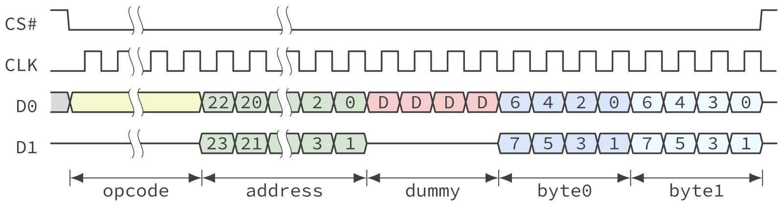
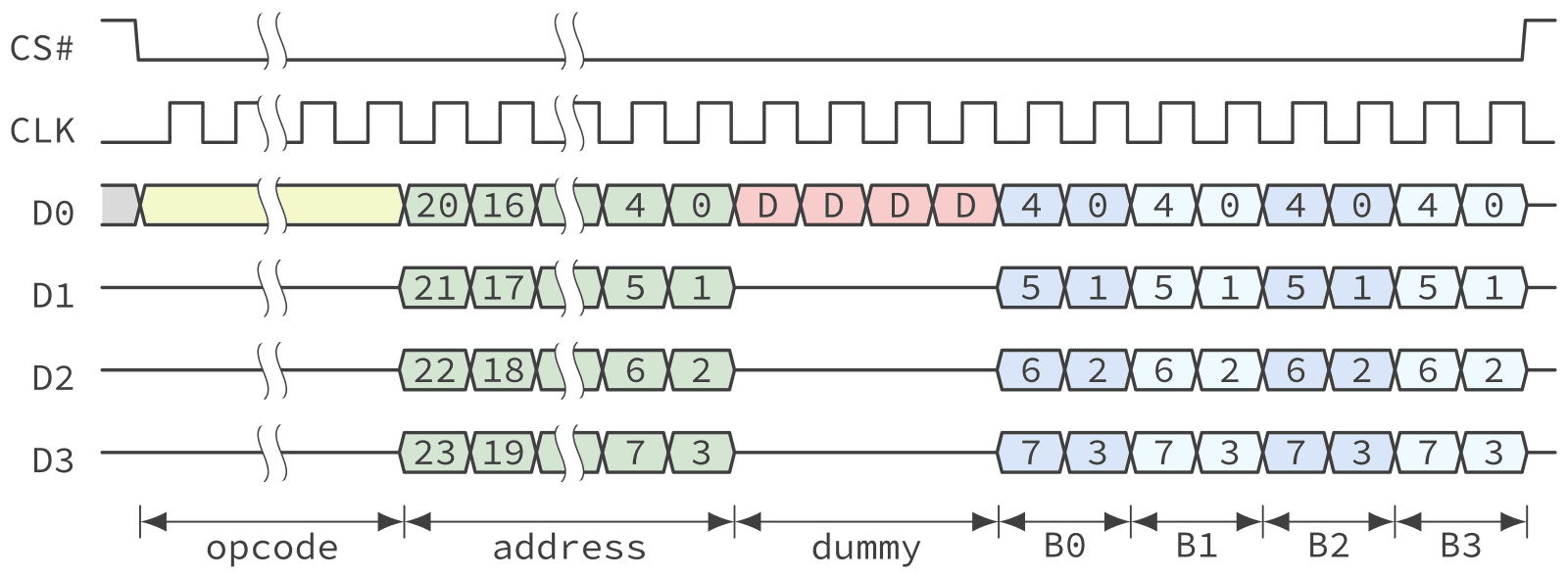
Dual (1-2-2) and Quad I/O (1-4-4)
Dual and Quad I/O modes, also known as DIO and QIO, goes further than the previous dual and quad SPI modes by transferring the address using two or four lanes. Note that the technique has some diminishing returns since additional dummy cycles are necessary to give the device enough time to prepare the read data. That being said, the overall latency is reduced since the device is given the page address a little bit sooner. Figure 8 and Figure 9 show examples of the DIO and QIO protocols.
Quad Peripheral Interface (4-4-4)
The Quad Peripheral Interface mode or QPI reduces the protocol overhead even further by also transferring the opcode using four lanes. Compared to all the other modes there is no 2 lane equivalent of QPI. By using the QPI mode, every instruction can be sent in two cycles saving 6 cycles of overhead without having to increase the number of dummy cycles.
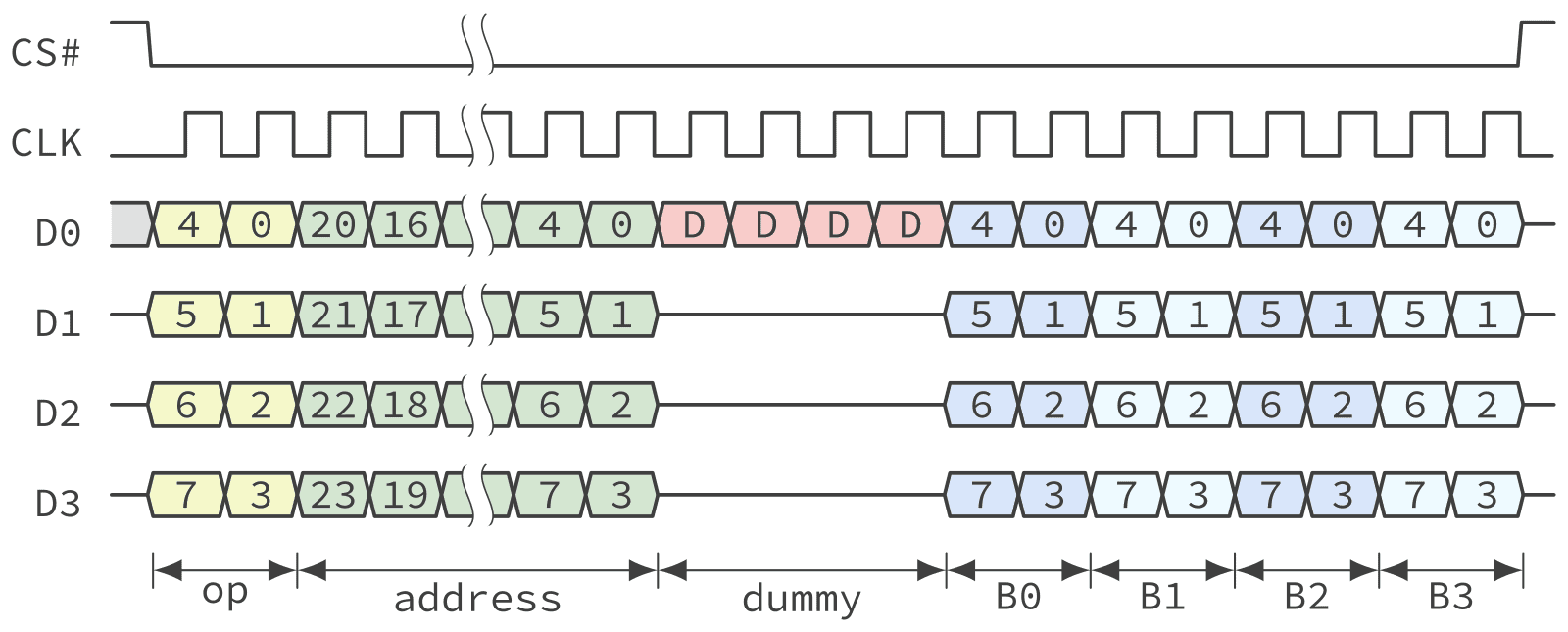
QPI is a bit rarer than the other modes and not all device families support it. Also QSPI controllers that support QPI mode are less common compared to all the other protocol variations discussed previously.
Dual Data Rate
Dual Data Rate (DDR) also known as Dual Transfer Rate (DTR) doubles the transfer speed by transmitting data on both the rising and falling edges of the clock. However, QSPI devices running in DDR mode usually do so at reduced maximum frequency. This means that DDR operation often does not translate in double the maximum read bandwidth. DDR mode is, however, useful to reduce the maximum frequency of the clock signal for the same performance thus simplifying board layout, reducing EMI etc.
In DDR mode the address and data are transferred as DDR signals but the opcode is still sent as a single data rate (SDR) signal like the other non-DDR modes. On chips that support DDR operation it is often, but not always, available for single, dual and quad operations. Some QSPI NOR devices, however, only supports DDR in 4-lane mode.
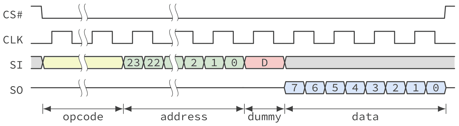
Figure 11 above presents an example of DDR operation for the single-lane mode. The protocol looks similar but notice that the clock alignment with the address and data bits. When running in DDR mode the first bit of address and the first bit of data will always happen on a rising edge. This means that the dummy cycles must still be full-clock cycles spanning a multiple of rising and fall edges. This can cause some confusion for devices or controllers that specify dummy cycles in bits or bytes since in DDR mode a bit length is half a dummy cycle.
Accelerated Read or XIP mode
QSPI NOR devices are often used for read-only applications in memory mapped mode. And when the program instructions are executed directly from the flash memory, this is known as Execute in Place or XIP mode. To reduce the latency of those reads even further most devices have an accelerated read mode where the opcode is no longer needed and the address can be sent immediately after the chip select is asserted. The exact protocol to be used must be agreed upon between the QSPI controller and the QSPI device prior to entering the accelerated read mode.
Dual-Quad / Twin Quad
Some QSPI controller supports accessing two flash devices in parallel. This is often called a dual-quad configuration. This mode only adds 4 pins to the design since the chip select and clock pins can be shared. To go with this feature manufacturers also offer dual-die devices designed for this sort of operation. These dual-quad or twin-quad devices are usually only offered for large capcity devices from 1 Gbit in size and over.
Beyond QSPI: OctoSPI, Octal SPI, OctaBus, Xccela and HyperBus
There comes a point where there’s a limit to how much performance can be squeezed out on one type of bus. There are, however, multiple device family boasting an 8-lane version of the QSPI protocol which in theory gives double the bandwidth of an equivalent QSPI memory. Those devices also goes further than that by adding a data strobe from the device back to the host. This improves the ability of the host’s controller to centre the sampling point with the data eye at high clock rate. With this addition, NOR Flash memories can reach read bandwidth up to 400 and even 500 MiB/s, considerably higher than any existing QSPI devices.
Application Level Considerations
After reading this article, one might be overwhelmed trying to select the highest performance combination of QSPI controller and QSPI memory devices. However, that choice must be placed in the context of the application’s requirements. Read performance and read latency is paramount for execute in place (XIP) operation in which case the NOR device will be used for read-only and probably in an accelerated read mode where the opcode is not necessary. This makes the somewhat rarer QPI mode rather unnecessary since the opcode won’t be transmitted anyways.
When using a file system things are a little different. With a mix of reads and writes the overall performance will be dominated by the relatively slow erase and programming speed of NOR Flash memory. Even for a read intensive application it would take a very fast application class processor to be able to read and process data as fast as it can be read from the Flash. As such, attaining the lowest operation latency and highest bandwidth may not be necessary, especially on slower MCU. This helps broaden the choice of devices, reduce cost and potentially lower the power usage by running at a lower serial clock frequency.
Conclusion
Readers brave enough to have read up to this point should now have a solid understanding of most variations of the QSPI protocol. Again, when trying to optimize performance, it cannot be stressed enough that the choice of device can be affected by the chosen MCU or SoC and more importantly by the application’s requirements. Different use cases and memory access patterns may call for different device features while in some cases may make some higher cost devices unnecessary.
The next article will focus on the QSPI NOR command set and device configuration.
Click here to go to the first article in the series.
If you have any questions or would like some guidance about selecting the best flash device or file system for your application please do not hesitate to contact us.