
Why use serial NAND over serial NOR? Picture this. You are on the verge of sending an ambitious design out for production. As the project comes to an end, you should feel a sense of victory. Instead, the atmosphere is tense. You should have known that 128Mbit of data storage would be too tight. Your heart is racing. NOR Flash memory with higher capacities are not available in the same 8-pin package. And the cost is much higher. As a PCB redesign seems inevitable, NAND Flash furtively appears as a cheaper alternative. But your MCU does not feature the needed parallel memory controller. As you are picturing yourself in a downward spiral of routing mazes and bit-banging madness, you wake up. What a horrible nightmare.
Fortunately, if this were to happen in real life, you would be covered. How? Thanks to Serial NAND Flash, also known as QSPI NAND Flash or even SPI NAND, a memory technology specifically designed as a direct alternative to its popular cousin, Serial QSPI NOR. Don’t be misled by this premise though: Serial NAND is a very capable storage solution and a perfectly valid choice on its own. But what exactly is Serial NAND? How does it compare to QSPI NOR? How does it compare to parallel NAND? This is what this article is all about.
An Alternative to Serial QSPI NOR
Modern Flash memory technologies cover a wide spectrum of densities and performances. Taken as a whole, these technologies are capable of supporting an equally wide array of embedded applications. But migrating from one technology to another comes with abrupt changes in cost, energy consumption, performance, error management, package, and so on.
From an application engineering perspective, this is bad. Life would be easier if we could freely move across the full spectrum of available technologies as the design progresses, and postpone definitive decisions until as late as possible.
Serial NAND goes some way towards that ideal. It’s not perfect — in particular, it focuses on the lower end of the capacity range (roughly up to 4Gbit) — but it does provide a smoother transition path between NOR and NAND technologies. Let’s see how.
Common external features
Using the industry-standard QSPI bus, common packages (e.g. 8-pin SOIC or DFN/SON and 16-pin SOIC) and a fully compatible pinout, QSPI NOR and NAND technologies can be supported with a single board design. This largely reduces the costs and risks associated with either maintaining different board designs, or making the definitive choice of storage technology early on in the design process.
Similar Command sets
Without being identical, the Serial NAND command set mimics that of QSPI NOR. From a software perspective, this makes porting easier. This strategy also helps preserve the compatibility with some QSPI controllers that are command-aware. Command set compatibility is not perfect, though. Read accesses to Serial NAND, for instance, are made of two separate commands — one for loading the data from the flash array into a read buffer, and another one to transfer the data from the buffer to the host — whereas there is no loading phase on QSPI NOR. If you consider Serial NAND for your application, make sure to read your QSPI controller documentation to avoid bad surprises.
Transparent error management
Built-in ECC is a critical feature of Serial NAND with regard to NOR compatibility. Indeed, the vast majority of QSPI NOR memories do not require error correction. And although most low-end processors feature a QSPI controller, very few have the hardware acceleration needed to perform ECC calculations without hindering overall write performances. Built-in error correction is possible because Serial NAND is based on the single-level cell technology (SLC NAND) which exhibits very low intrinsic error rates. As a result, basic error correction schemes (often only 1-bit ECC per 512 bytes) are enough to meet expected reliability levels. By contrast, the multi-level cell technology (MLC NAND) requires much stronger algorithms (40-bit ECC per 1024 bytes is not unusual) which are best implemented on the controller side.
Obviously, intrinsic differences between NOR and NAND remain despite the functional resemblance of their respective QSPI implementations. The combined erase/write energy consumption of NOR flash, for instance, is roughly 100 times that of NAND. There is no way around that. Read granularity is another example. NOR allows for byte-level accesses while NAND is limited to whole pages. And while Serial NAND features built-in error correction, software remains responsible for managing bad blocks.
If your application heavily depends on such specificities, then there is no alternative: it’s either NOR or NAND (or whatever else fits your application). Otherwise, QSPI devices go a long way towards blurring the boundaries between storage technologies. NOR and NAND, of course, but also technologies like MRAM, FRAM and nvSRAM.
A More Accessible Form of SLC NAND
Through its serial interface and built-in error management, Serial NAND provides a near drop-in alternative to QSPI NOR. But it doesn’t stop there. Serial NAND is a very compelling solution in its own right. It makes the unique benefits of the NAND flash technology accessible to a vast middle-ground class of applications for which balance is key. Indeed, Serial NAND is based on SLC NAND, a storage technology known for offering one of the best overall trade-offs between competing characteristics such as cost, capacity, reliability and energy consumption. Let’s try to put numbers on this.
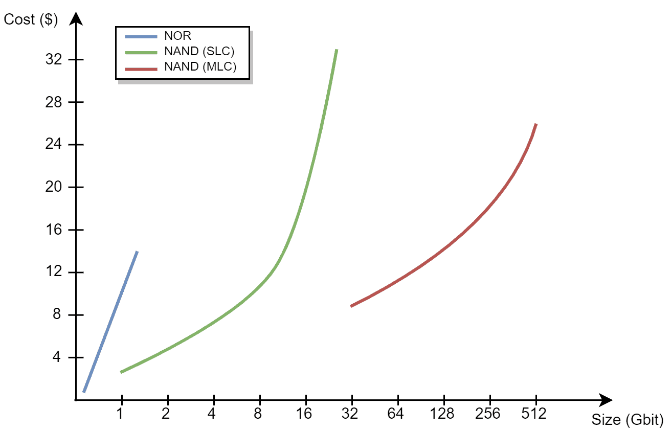
Cost versus capacity
The following figure shows how cost increases as we move from lower to higher storage capacities. Although NOR is the absolute cheapest solution for small capacities, SLC NAND quickly makes more economical sense as capacity requirements increase beyond 128Mbit or so.
As the capacity shifts towards a few gigabits, MLC NAND eventually appears as a better deal. But MLC NAND requires stronger error correction algorithms. Meeting this requirement typically involves more capable and more expensive memory controllers. Taking that into account, SLC NAND remains one of the cheapest solution per byte, especially in the neighborhood of 1Gbit which is quite usual for deeply embedded applications.
Endurance
As memory density increases, endurance goes down. Endurance is usually expressed as the number of erase cycles beyond which retention and error rate guarantees do not hold anymore. For NOR and SLC NAND flash, this number is roughly the same (around 100000). For MLC NAND, it drops to 10000 and sometimes less.
Higher endurance obviously means extended lifetime. It also means less pressure on wear-levelling algorithms, error correction and, in a broader sense, all mechanisms involved in end-of-life management. By nature, these algorithms are complex, as they involve various software and hardware components, and difficult to test. From that perspective, it is a sensible design approach to choose a flash technology, like SLC NAND, whose life expectancy extends well beyond that of the whole system.
Interestingly, endurance can also be traded off against increased write performances, by introducing extra degrees of freedom in the design of wear-leveling algorithms — usually in the form of higher tolerances on erase cycling variations between flash blocks.
Read/Write throughput
NAND flash (both SLC and MLC) delivers much higher raw write speeds than NOR flash. On Serial NAND for instance, sustained write throughput can easily exceed 5MBytes/s. On NOR flash, it’s 10 times less. With regard to read performances, it’s the other way around. Besides, NOR flash features a finer read access granularity, which further enhances net read performances over NAND.
Interestingly, using a proper log-structured file system, access size has only a limited impact on overall write amplification and net write performances, even as the access size drops below the page size. So, although NOR flash provides a finer write access granularity, it does not necessarily translate into tangible benefits with regard to net write performances (more on raw versus net performances in articles to come).
Energy consumption
Flash programming current remains fairly constant (roughly around 25 mA) throughout the various technologies (NOR, SLC NAND and MLC NAND). As a result, the technology with the lowest program time also has the lowest energy consumption. In particular, NOR and NAND technologies differ by 2 orders of magnitude. With regard to read operations, energy consumption is much lower, both for NAND and NOR technologies. Because overall read amplification tends to be lower on NOR flash, read energy consumption also tends to be lower.
Available Serial NAND Devices
Serial NAND chips are available from multiple Flash manufacturers, and since this article was first written, many product families reached the market further increasing the available choices, including the Winbond W35 QspiNAND and W35 OctalNAND devices, Macronix MX35 Serial NAND portfolio as well as the Micron MT29 Serial NAND product series.
The Importance of the File System
To be successful, however, it is imperative that the technology chosen for a design is well supported by the software. As described in detail in our article What is a Flash File System, a file system designed with support for NAND Flash memory is a necessity to enable Serial NAND memory in a design. The chosen file system must not only be able to handle all the requirements that were present for NOR Flash, such as wear-levelling and block erase, it must also be able to handle ECC error recovery and bad block management.
In addition to the Flash specific requirements, an embedded application warranting the use of Serial NAND probably has important performance and resource requirements as well. NAND devices being usually larger than NOR devices means a file system might require additional RAM for caching or for internal data structures. Similarly, bad block management and the heightened reliance on wear-levelling by NAND technology means that some file system may scale badly on Serial NAND compared to Serial NOR. Our article about Choosing an Embedded File System goes over many of those important considerations.
A Word on RAM-like Technologies
Because they also come as QSPI devices, let’s take a moment to discuss RAM-like technologies. As their name implies, RAM-like technologies refer to storage technologies featuring the same random access characteristics as volatile RAM. MRAM and FRAM are arguably the most prominent members of this category. These technologies feature extremely high read/write speeds. Besides, unlike flash memory, MRAM and FRAM technologies don’t require charge pumps for writing. It translates into lower and near-symmetrical energy consumption between read and write operations.
However, their capacity range does not extend beyond a few megabits and their cost per byte is prohibitively high for most applications. Besides, despite raw access speeds beyond 50MByte/s, net performances will realistically remain much lower as other bottlenecks are revealed (limited rate of data production, finite processing power, file system overhead).
Overall, RAM-like technologies are best suited for niche designs where absolute performance is the crux. In comparison, SLC NAND (and thus QSPI NAND) stands as a much more balanced solution for general-purpose applications.
What’s Next?
As we have seen, serial NAND Flash is a versatile storage solution that can benefit application designers in two different ways: as a near drop-in replacement for QSPI NOR and as a more accessible, easier to integrate form of SLC NAND for deeply embedded designs. Like anything else, it’s not perfect. It requires bad block management, for instance, whereas NOR flash doesn’t. It’s certainly not as fast as RAM-like technologies and MLC NAND offers far greater density. Yet, it offers a balanced trade-off between cost, board estate, energy consumption, performances and reliability. In that regard, it remains a very relevant response to many embedded storage challenges.
Stay tuned as we continue our discussion with an in-depth analysis of TSFS over Serial NAND benchmarking results in articles to come. In the meantime, thank you for reading. If you have any questions regarding the Serial NAND technology or any other embedded-related topic, please feel free to reach out to us.