Following last Spring’s introduction of their new lineup of xSPI STT-MRAM, Everspin Technologies has just announced that the EMxxLX family of products is now ready for production. As we had the chance of getting hold of a sample beforehand, we thought it would be interesting to put it to the test and let you know our first impressions.
For this article, we look at Everspin’s EM064LX in the context of data storage applications, focusing on access speed metrics, that is, average throughput and worst-case access latency. For context, we compare MRAM performances with NOR and NAND flash using a simple benchmark and discuss the implications of the obtained results from an application design standpoint.
Overview
Before we jump into the actual benchmark, let’s first reiterate the main general benefits of the EMxxLX product family. The first and most prominent benefit is speed. The EMxxLX lineup supports read and write accesses at bus speed, which can go as high as 400 MB/s in octal DTR configuration. Whether or not this speed can be achieved in practice largely depends on the host processor performances. Still, even in the more common (for deeply embedded applications anyway) and conservative Quad SPI configuration, we have obtained symmetrical read/write speeds approaching 60 MB/s, a far cry from typical NOR and NAND performances.
Another obvious benefit of MRAM is its low energy consumption. From the EM064LX datasheet, the active write current is 155 mA in a DTR octal configuration and a clock speed of 200 MHz. A quick back-of-the-envelope calculation yields a write energy of 0.155 A x 1.8 V / 400 MB/s = 0.7 nJ per byte. This is roughly 10 times less than NAND and 200 times less than NOR.
Finally, MRAM is characterized by virtually unlimited endurance which greatly simplifies software design. Let’s recall that the memory endurance is the number of program/erase cycles that can be performed while maintaining a set of original specifications such as maximum error rate and load/program/erase time. Limited endurance is one of the main reasons for flash management software complexity. At the file system level, wear-levelling algorithms are needed to make sure that write operations are evenly spread across all blocks. This is crucial to prevent blocks from prematurely wearing out, eventually making the whole device unusable. At a higher level, limited endurance must be dealt with from early design stages to validation and beyond, with diagnostic tools to monitor the device once in the field. This equally applies to bare flash and managed flash memories.
Benchmark
We now expose access throughput and latency disparities between MRAM and flash memory through a simple benchmark.
Methodology
We use three different memory devices for the purposes of our performance comparison, namely the Everspin EM64LX 64 Mib STT-MRAM, the Micron MT25Q 128 Mib NOR flash and the Micron MT29F 1Gib SLC NAND flash.
For each device we read/write 64 MiB worth of data, starting at address 0 and wrapping around at address 8388608 (8 MiB). We repeat the process for various access sizes: 2 KiB, 4 KiB, 8 KiB, 16 KiB, 32 KiB and 64 KiB. On flash, each block is erased before its first page is written. The erase time is included in the write throughput measurements.
The benchmark runs on a STM32H755ZI, on the Cortex-M7 core clocked at 240 MHz. The Quad SPI bus is used in a 1-4-4 configuration (1 line for the command, 4 lines for the address and 4 bytes for the data) and is clocked at 120 MHz which is close to the maximum supported frequency of 133 MHz (the same for all three devices). Other than the memory driver, the benchmark code and configuration are exactly the same for all three devices.
Results and Discussion
Average Write Throughput. The average write throughputs obtained from the tested devices are shown in Figure 1. A few things immediately stand out. First and most obviously, MRAM write performances are approximately five times higher than NAND flash and two hundred times higher than NOR flash (hardly visible on the graph at around 280KB/s, independent of the access size).
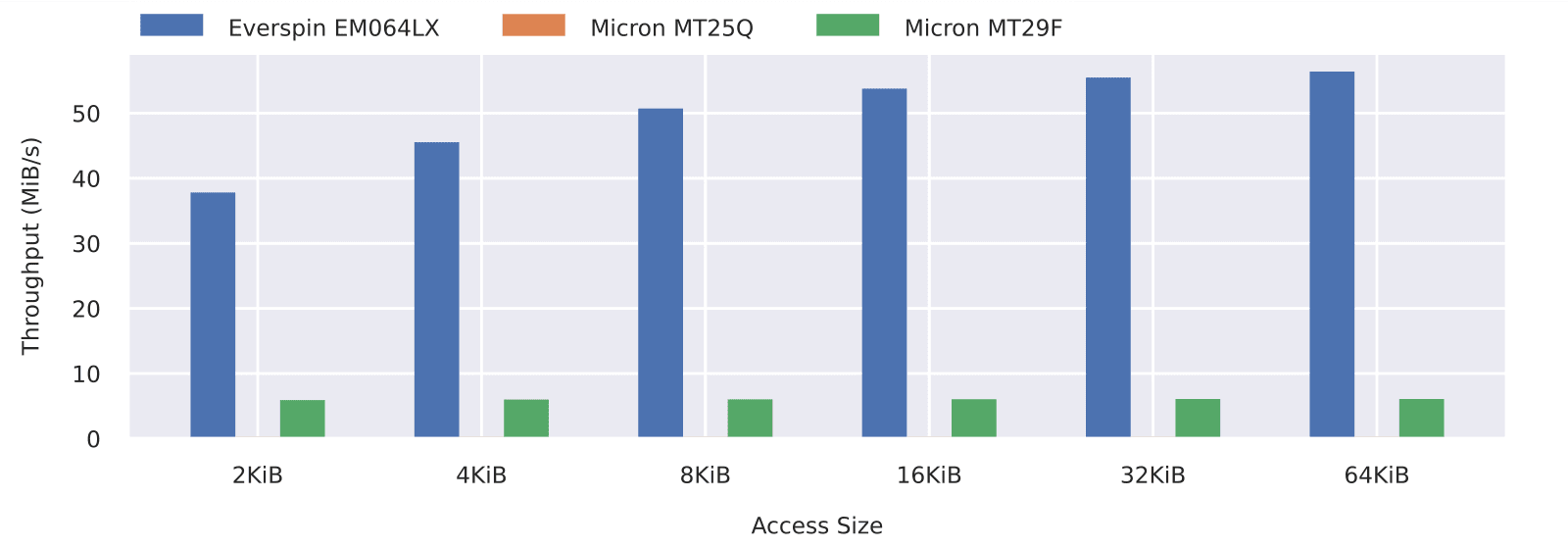
Looking at Figure 1 we can see how MRAM performances are CPU-bound. That is, for small accesses, the time spent in the driver code, in particular setting up the DMA for the requested transfer, is long enough compared to the actual transfer time, that it limits the overall throughput. This shows how data storage software challenges may shift in the future as raw device performances increase. With flash technologies, especially NOR flash, throughput optimization is mostly a matter of minimizing read and write amplification. The extra cost paid in CPU cycles is almost always worth it. This is clearly not the case for MRAM.
Average Read Throughput. The average read throughputs achieved for all tested devices are shown in Figure 2. This time, measurements are more alike across the different technologies. MRAM and NOR flash read speeds are in fact identical which makes perfect sense as both technologies support reading at bus speed. In both cases, throughput values asymptotically tend towards 60 MB/s as the access size increases and the relative access overhead correspondingly decreases.
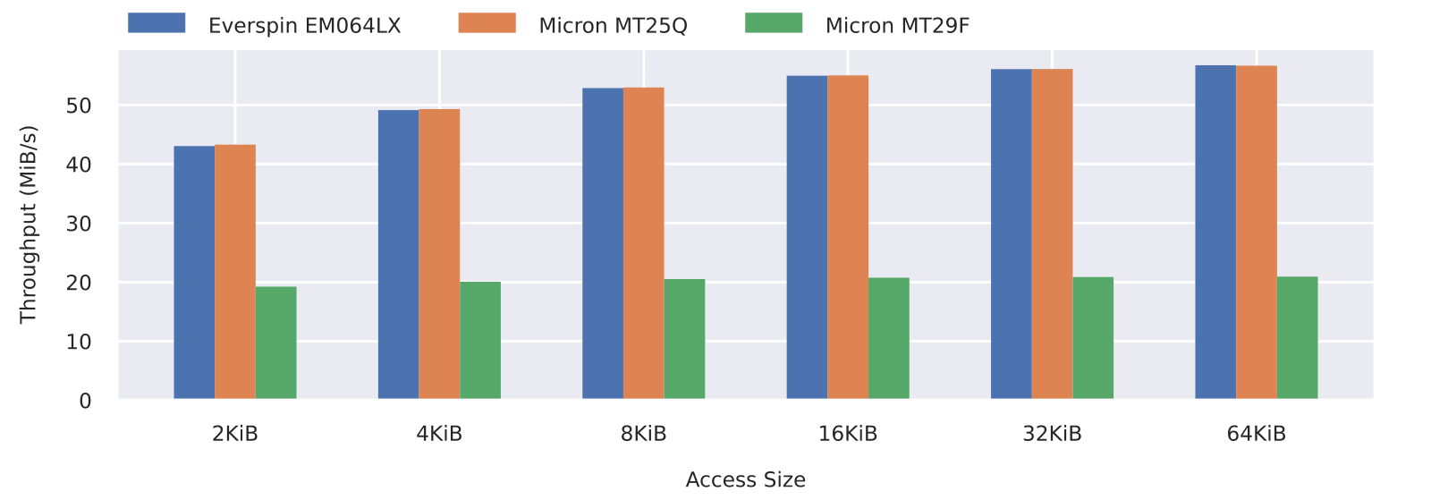
In the case of NAND flash, read performances are limited by the page load time which, according to the MT29F datasheet, is 70s with the ECC enabled. Higher throughputs could likely be achieved using more powerful, MCU-side ECC engines, but those are not so common these days. Another strategy for improving read performances on NAND flash is to take advantage of the pipeplining capabilities of the device, where data can be transferred from one internal buffer (the cache register) while the next page is loaded from the flash array to a separate buffer (the data register). Although this technique is quite effective, yielding (roughly) a 50% increase in read performance, this strategy only works for large read accesses and is not supported by all NAND flash devices.
Worst-Case Write Latency. The worst-case write latencies obtained for all tested devices are shown in Figure 3. For both NOR and NAND flash, the worst-case access time is dictated by the block erase time. The typical erase time is 150 ms for the MT25Q and 2 ms for the MT29F which matches the results shown in Figure 3. Note that these results can significantly degrade with wear, voltage and temperature. The maximum erase time is 1s for the MT25Q and 10 ms for the MT29F.
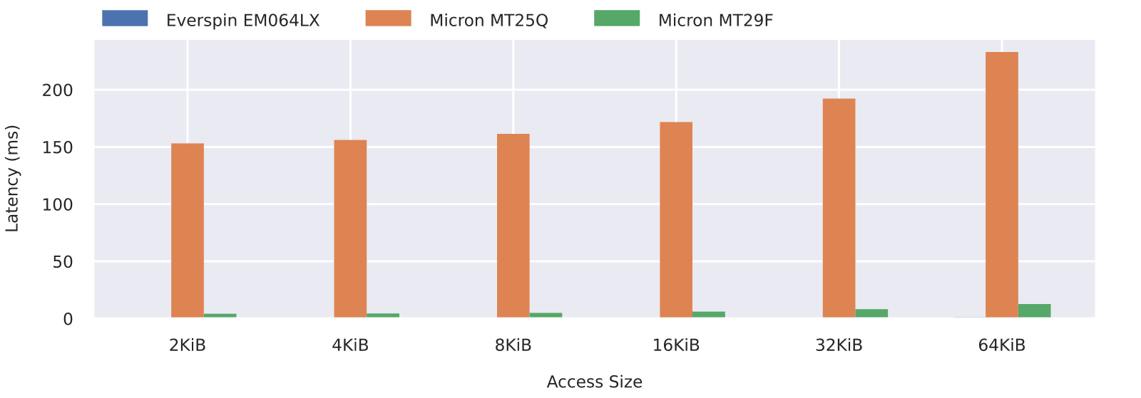
In the case of MRAM, there is no need for erasing, and write accesses can be performed at bus speed. The worst-case latency is thus not only low but constant for a given access size. This is a huge benefit from an application design standpoint, especially in terms of RAM usage.
To illustrate our point, consider a simple data logging application based on NAND flash (no file system, just raw device accesses for the sake of simplicity). Now, suppose that data is logged at a fixed interval. Make it 4 KiB of data every 1 ms. In terms of average throughput, this is 4 MB/s, comfortably under the measured 6 MB/s maximum throughput (see Figure 1). However, once every 32 accesses (one 128 KiB block divided by 4 KiB accesses), a used block must be erased. This typically takes 2 ms. During that time, incoming data cannot be written. Assuming that data loss is not acceptable, incoming data must be temporarily stored in RAM until the erase is done and write accesses can resume. In our example, 8 KiB of RAM would be needed, a significant amount for many embedded applications.
Note that our example purposely ignores many aspects of flash management and their impact on performance. Garbage collection alone often results in more latency than block erasing. Nevertheless, the example demonstrates the crucial relation between throughput, access time distribution and RAM usage. With that in mind, we can appreciate the practical implications of the EMxxLX lineup constant access time (for a given access size), in particular how the full throughput potential of the device can be reached with no buffering memory at all, further increasing its effective performance advantage over flash.
Conclusion
On paper, it was abundantly clear from the start that the EMxxLX lineup would outperform flash memory in almost every aspect. In this sense, we have only stated the evidence. Hopefully, though, we have also demonstrated the sheer magnitude of the performance gap between MRAM and flash, in particular in terms of access speed, and especially considering the relation between write throughput, write latency and RAM usage.
If you have any questions or would like some guidance about selecting the best flash device or file system for your application please do not hesitate to contact us.