In this article, we explain how to connect, configure and access a serial NAND device connected through SPI to the Nordic Semiconductor’s nRF5340 MCU. In the process, we discuss serial flash fundamentals, write a fully functional SPI flash driver, and compare SPI and QSPI performances.
For demonstration purposes, we use the nRF5340-DK development kit which is cheap and easy to obtain. We also use Zephyr OS for the demonstration, since it is a very popular choice on Nordic platforms, although most of the information equally applies to other RTOS/SDKs. The same goes for the choice of NAND device. We use the Micron’s MT29F1G01 QSPI NAND, but the provided driver code can be adapted to any serial flash device with only minor modifications.
It should be noted that Zephyr OS already comes with some support for serial NOR flash, including SPI and QSPI NOR drivers, a device-agnostic flash interface, and a small file system, LittleFS, which can be used for simple data storage needs (see our article Comparing Embedded File Systems for a comparative discussion of LittleFS). For higher performances, as well as for NAND flash support, third party solutions exist which we discuss in building a reliable storage stack.
A Word of Caution
Building a fast and reliable data storage solution based on raw NAND is within the reach of all embedded application developers. This is especially true for the serial SLC NAND flash variant with built-in ECC, which, in our opinion, is an underappreciated option. Be aware though that there is more to NAND-based storage than just writing a device driver. Although this article extensively describes how to connect, configure and access a raw NAND device, it does not cover, wear-levelling, bad block management, and other NAND management considerations. Unless you want to make a career out of data storage, these aspects are best handled by proven solutions, something that we discuss later on in the last section of this article.
Why SPI rather than QSPI?
There are many reasons for using raw SPI rather than QSPI. Some MCUs simply do not have a QSPI controller, which makes sense for low-power MCUs where cost effectiveness is more important than performance. This is the case, for instance, of the Silicon Labs Series 2 MCUs.
Another reason for using SPI over QSPI, is the fact that some QSPI controllers use hardwired, NOR-specific instructions that are incompatible with NAND devices. This is the case of the nRF MCUs. Also, in the particular case of the nRF5340, there is a number of QSPI-related errata which may be problematic for some applications.
Application constraints, like energy consumption, or board design, are yet more reasons why the use of a QSPI bus may be impossible or undesirable.
Hardware Setup
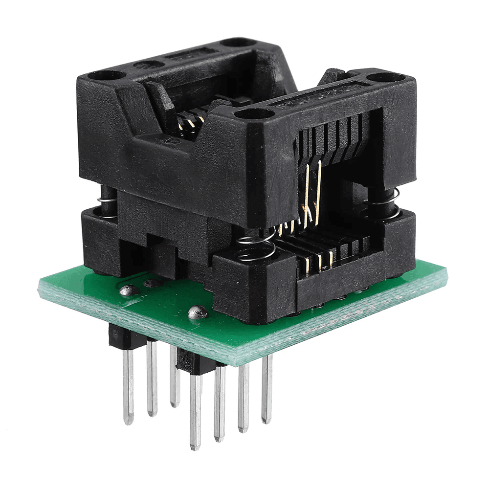
Connecting a serial flash to the nRF5340-DK through SPI could not be easier. In its simplest form, all it takes is a breadboard, a SOP/DIP programmer adapter and a few jumper wires. Flash programmer adapters such as the one shown in Figure 1 can be bought from various popular online retailers for SOIC8 (wide and narrow), SOIC16, and even BGA packages. Since the maximum SPI clock frequency on the nRF5340 is 32MHz, you can safely ignore impedance matching considerations, and other potential high-frequency bus issues, so long as you keep your connections reasonably short and tidy.
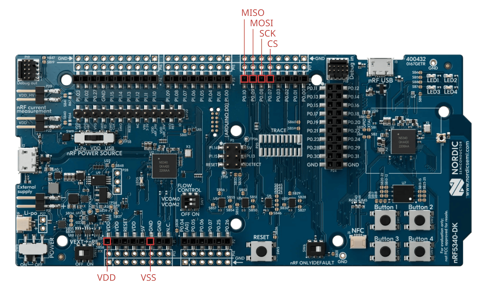
The nRF5340 has 5 SPI controllers but only the SPI4 controller can reach 32MHz through dedicated pins (others are limited to 8MHz). On the nRF5340-DK evaluation board, the SPI4 pins are available from the P6 external connector as shown in Figure 2. Note that the chip select pin was chosen for its physical proximity to other SPI pins, but any other available GPIO would do.
Zephyr SPI Configuration
In this section we show how to configure a Zephyr project and device tree to enable SPI communication. Obviously, these steps are very specific to Zephyr OS and the nRF5340 MCU. For other platforms or SDKs, most manufacturers provide at least one basic SPI example that you can use as a starting point.
The first step towards enabling SPI communication is to enable the SPI module, and specifically the SPI4 controller on the nRF5340. This is done by setting the CONFIG_SPI and CONFIG_NRFX_SPIM4 configurations in the project configuration file (i.e. prj.conf) as shown in Listing 1. We also enable the GPIO module for the chip select through the CONFIG_GPIO and CONFIG_GPIO_NRFX configurations.
CONFIG_GPIO=y
CONFIG_GPIO_NRFX=y
CONFIG_SPI=y
CONFIG_NRFX_SPIM4=y
Listing 1 – Configurations to be added to the project configuration file to enable
The next step is to configure the pin mux for the SPI4 controller. This can be done through a device tree overlay (i.e., app.overlay) as shown in Listing 2. Again, we use P0.07 for the chip select here, but you can choose any other available GPIO instead.
&pinctrl {
    spi4_default: spi4_default {
        group1 {
            psels = <NRF_PSEL(SPIM_SCK, 0, 8)>,
                    <NRF_PSEL(SPIM_MISO, 0, 10)>,
                    <NRF_PSEL(SPIM_MOSI, 0, 9)>;
            nordic,drive-mode = <NRF_DRIVE_H0H1>;
        };
    };
    spi4_sleep: spi4_sleep {
        group1 {
            psels = <NRF_PSEL(SPIM_SCK, 0, 8)>,
                    <NRF_PSEL(SPIM_MISO, 0, 10)>,
                    <NRF_PSEL(SPIM_MOSI, 0, 9)>;
            nordic,drive-mode = <NRF_DRIVE_H0H1>;
        };
    };
};

&spi4 {
    cs-gpios = <&gpio0 7 GPIO_ACTIVE_LOW>;
};
Listing 2 – Device tree overlay for SPI4 controller and chip select
Once the device tree is appropriately set, the device structure for the SPI4 controller, as well as the spec structure for the chip select pin can be accessed using dedicated macros as we will show later on.
Serial Flash Commands
Before we start coding anything, let’s hit pause for a moment and explain how the host MCU communicates with the external serial flash device. If you already are familiar with serial flash devices, feel free to skip to the next section.
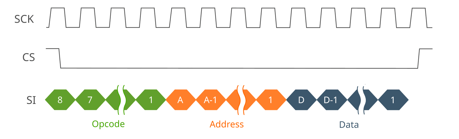
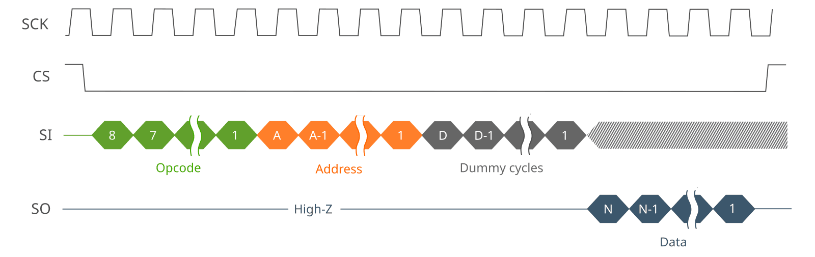
The host MCU controls and accesses the external flash by sending commands, most often through SPI or QSPI. There are commands for reading and writing data, reading status registers, writing control registers, resetting the device, erasing blocks, and so on. Some commands are common to all flash devices, others are specific to one type of flash, or even to one particular device. Regardless, each command is made of only three phases: the opcode, address and data phases. The opcode phase starts every command sequence (except in XIP mode which we can ignore here). The address and data phases are optional.
For reference, Table 1 lists some command definitions that we will use later on when we write the device driver. On the SPI bus, data write and data read commands look something like Figure 3 and Figure 4 respectively. Other commands look essentially the same, possibly minus the address and data phases depending on the particular command.
| Command | Flash Type | Opcode | Address bytes | Data bytes | Dummy cycles |
|---|---|---|---|---|---|
| WRITE ENABLE | NOR/NAND | 0x6 | 0 | 0 | 0 |
| BLOCK ERASE | NOR/NAND | 0xD8 | 3 | 0 | 0 |
| PAGE PROGRAM | NOR | 0x2 | 3 or 4 | 1 to N | 0 |
| PROGRAM LOAD | NAND | 0x2 | 3 | 1 to N | 0 |
| PROGRAM EXECUTE | NAND | 0x10 | 3 | 0 | 0 |
| READ | NOR | 0x3 | 3 or 4 | 1 to N | 0 |
| FAST READ | NOR | 0xB | 3 or 4 | 1 to N | 1 to D |
| READ FROM CACHE | NAND | 0x3 | 2 | 1 to N | 8 (1 byte) |
| PAGE READ | NAND | 0x13 | 3 | 0 | 0 |
| READ STATUS | NOR | 0x5 | 0 | 1 | 0 |
| GET FEATURES | NAND | 0xF | 1 | 1 | 0 |
| READ ID | NOR | 0x5 | 0 | 3 | 0 |
Notice that, in some cases, extra wait (or dummy) cycles must be inserted between the address and data phases. This is the case for the NOR flash FAST READ command, which allows for higher clock frequencies at the cost of a higher latency. This is also the case for the NAND flash READ FROM CACHE command, which requires 1 dummy byte, or 8 cycles in an SPI bus configuration.
Command Handling
Since all serial flash commands share the same structure, command handling and writing on the bus can be done in a device-agnostic sublayer, separate from the actual device driver. In that case, the device driver remains responsible for command definitions, timings, register definitions, and other device-specific considerations.

This layered approach is depicted in Figure 5. It makes writing a new device driver much easier. Also, the same device driver can be reused over SPI, QSPI, or any other communication protocol, simply by replacing the command handling layer. The same goes for porting to another RTOS or SDK.
Listing 3 shows a minimal implementation of the spi_flash_xfer() function at the heart of our command handling driver sublayer. Listing 4 shows the corresponding header file. The function has two parameters. The first is the flash instance which contains all the structures required by the Zephyr SPI interface. The second parameter is a command descriptor which contains the opcode, address, address width, data, data length, number of dummy cycles, and access direction.
The address width is either 2, 3 or 4-byte wide depending on the flash device and the addressing mode in use. Notice in Listing 3 how the address bytes are reordered such that the MSB is sent first, which is required for most (if not all) serial flash devices. By the way, the bit order is also from most significant to least significant. This is the default for most SPI controllers, but if you use a different setup, you might want to verify that this is indeed the case.
Another thing to notice is how dummy cycles are handled. Dedicated QSPI controllers generally support arbitrary numbers of dummy cycles, but most SPI controllers (like the nRF5340 SPI controller) do not. Instead dummy cycles are generated by reading or writing dummy bytes, which means that the number of dummy cycles must be a multiple of 8. Importantly, the driver cannot simply round up the requested number of dummy cycles without changing the flash device configuration accordingly. In the case of serial NAND devices, the number of dummy cycles is always a multiple of 8, so this is not an issue anyway. In the case of serial NOR devices however, this is something to keep an eye on. In Listing 3, we simply assert that the requested number of dummy cycles is indeed a multiple of 8, leaving the responsibility of properly configuring the bus and flash device to the caller if need be.
#include <stdint.h>
#include <stdio.h>
#include <stdbool.h>

#include <zephyr/drivers/gpio.h>
#include <zephyr/drivers/spi.h>

#include "spi_flash_driver.h"

// SPI flash transfer implementation.
int spi_flash_xfer(const spi_flash_t *p_flash, const spi_flash_xfer_t *p_xfer)
{
    struct spi_buf spi_buf;
    const struct spi_buf_set spi_buf_set = { .buffers = &spi_buf, .count = 1u};
    int res;

    // Assert chip select.
    res = gpio_pin_set_dt(p_flash->p_cs_gpio_dt_spec, 1);
    if (res != 0) return (res);

    // Send the opcode.
    spi_buf.buf = (void *)&p_xfer->opcode;
    spi_buf.len = 1;
    res = spi_write(p_flash->p_spi_dev, p_flash->p_spi_cfg, &spi_buf_set);
    if (res != 0) return (res);

    // Send the address if required.
    if (p_xfer->addr_width > 0u) {

        uint8_t t_addr[4];

        // The address is either 2, 3 or 4-byte long.
        if ((p_xfer->addr_width < 2u) || (p_xfer->addr_width > 4)) {
            return (-1);
        }

        // Address is sent MSB first.
        for (size_t k = 0u; k < p_xfer->addr_width; k++) {
            t_addr[p_xfer->addr_width - k - 1] = (p_xfer->addr >> (k * 8u)) & 0xFF;
        }
        spi_buf.buf = &t_addr[0];
        spi_buf.len = p_xfer->addr_width;
        res = spi_write(p_flash->p_spi_dev, p_flash->p_spi_cfg, &spi_buf_set);
        if (res != 0) return (res);
    }

    // Send dummy cycles if required.
    if (p_xfer->dummy_cycle_count > 0) {

        uint32_t cycle_ctr;
        uint8_t byte = 0;

        // The dummy cycle count must be a multiple of 8.
        if (p_xfer->dummy_cycle_count % 8u != 0) {
            return (-1);
        }
        cycle_ctr = 0u;
        while (cycle_ctr < p_xfer->dummy_cycle_count) {
            spi_buf.buf = &byte;
            spi_buf.len = p_xfer->dummy_cycle_count / 8u;
            res = spi_write(p_flash->p_spi_dev, p_flash->p_spi_cfg, &spi_buf_set);
            if (res != 0) return (res);

            cycle_ctr += 8u;
        }
    }

    // Send data if required.
    if (p_xfer->data_len > 0) {
        spi_buf.buf = p_xfer->p_data;
        spi_buf.len = p_xfer->data_len;
        if (p_xfer->is_write) {
            res = spi_write(p_flash->p_spi_dev, p_flash->p_spi_cfg, &spi_buf_set);
            if (res != 0) return (res);
        }
        else {
            res = spi_read(p_flash->p_spi_dev, p_flash->p_spi_cfg, &spi_buf_set);
            if (res != 0) return (res);
        }
    }

    // Deassert chip select.
    res = gpio_pin_set_dt(p_flash->p_cs_gpio_dt_spec, 0);
    if (res != 0) return (res);

    return (0);
}
Listing 3 – SPI flash driver implementation.
#ifndef SPI_FLASH_DRIVER_H
#define SPI_FLASH_DRIVER_H

#include <zephyr/drivers/gpio.h>
#include <zephyr/drivers/spi.h>

typedef struct spi_flash {
    const struct device *p_spi_dev;
    const struct spi_config *p_spi_cfg;
    const struct gpio_dt_spec *p_cs_gpio_dt_spec;
} spi_flash_t;

typedef struct spi_flash_xfer {
    void *p_data;
    size_t data_len;
    uint32_t addr;
    uint8_t addr_width;
    size_t dummy_cycle_count;
    uint8_t opcode;
    bool is_write;
} spi_flash_xfer_t;

int spi_flash_xfer(const spi_flash_t *p_flash, const spi_flash_xfer_t *p_xfer);

#endif
Listing 4 – SPI flash transfer header
Writing the MT29F Device Driver
We can now start coding the actual device driver. As a reminder, we specifically target the Micron MT29F1G01 QSPI NAND but the driver can be adapted to any serial NAND device with only minor modifications, mostly in the setup phase and ECC handling code.
Let’s start with the device setup. Table 2 shows a minimal setup implementation. The setup phase does essentially two things:
- disable the write protection;
- enable the built-in ECC;
both of which may or may not be enabled by default depending on the particular MT29F variant. The built-in ECC is a necessity whenever the host MCU does not feature ECC acceleration, which is only the case for a few high-performance SoCs. Using software ECC, while possible in theory, would be overwhelming for a modest CPU like the nRF5340’s 128MHz Cortex-M33, especially given modern correction code requirements.
Another thing that you might want to do during the setup phase (which we do not do here) is to fetch the NAND parameter page. The parameter page contains many device-specific parameters like the number of planes, the number of blocks per plane, the number of pages per block, the page size, the error correction requirements, and so on. The parameter page is laid out in a standardized way, such that the information can be accessed without any prior knowledge of the connected device. We purposely skip that step in Listing 5 for simplicity and because it is perfectly fine to ignore the parameter page if you only plan on using a single device (which parameters you know in advance). If you were to design a generic driver though, this is how you would do it.
#define MT29F_OP_READ_ID           (0x9F)

#define MT29F_MANUF_ID             (0x2C)
#define MT29F_FEAT_ADDR_BLK_LOCK   (0xA0)
#define MT29F_FEAT_ADDR_CONFIG     (0xB0)

#define MT29F_CONFIG_REG_ECC_EN    (1<<4)

int mt29f_setup(spi_flash_t *p_spi_flash)
{
    spi_flash_xfer_t xfer;
    uint8_t t_buf[2];
    uint8_t dev_id;
    uint8_t manuf_id;
    uint8_t config;
    int res;

    memset(&xfer, 0u, sizeof(xfer));
    xfer.opcode = MT29F_OP_READ_ID;
    xfer.dummy_cycle_count = 8u;
    xfer.data_len = 2u;
    xfer.p_data = &t_buf[0];
    res = spi_flash_xfer(p_spi_flash, &xfer);
    if (res != 0) return (MT29F_ERR_IO);

    manuf_id = t_buf[0];
    dev_id = t_buf[1];

    // Make sure that the manufacturer ID is indeed Micron's.
    if (manuf_id != MT29F_MANUF_ID) {
        return (-1);
    }

    // Unlock blocks and disable write protect.
    res = mt29f_feat_set(p_spi_flash, MT29F_FEAT_ADDR_BLK_LOCK, 0x82);
    if (res != 0) return (res);

    // Modify the configuration register to enable ECC.
    res = mt29f_feat_get(p_spi_flash, MT29F_FEAT_ADDR_CONFIG, &config);
    if (res != 0) return (res);

    config |= MT29F_CONFIG_REG_ECC_EN;
    res = mt29f_feat_set(p_spi_flash, MT29F_FEAT_ADDR_CONFIG, config);
    if (res != 0) return (res);

    return (MT29F_ERR_NONE);
}
Listing 5 – MT29F driver setup implementation.
For reference, the mt29f_feat_get() and mt29f_feat_set() implementations used in the setup phase, are given in Listing 6 and Listing 7 respectively. Also, the MT29F SPI driver header file, which contains error code definitions and function prototypes, is given in Listing 8.
#define MT29F_OPCODE_FEAT_GET      (0x0F)

int mt29f_feat_get(spi_flash_t *p_spi_flash, uint32_t addr, uint8_t *p_reg)
{
    spi_flash_xfer_t xfer;
    int res;

    xfer.opcode = MT29F_OPCODE_FEAT_GET;
    xfer.addr = addr;
    xfer.addr_width = 1u;
    xfer.dummy_cycle_count = 0u;
    xfer.data_len = 1u;
    xfer.p_data = (void *)p_reg;
    res = spi_flash_xfer(p_spi_flash, &xfer);
    if (res != 0) return (MT29F_ERR_IO);

    return (MT29F_ERR_NONE);
}
Listing 6 – MT29F driver feature get implementation.
#define MT29F_OPCODE_FEAT_SET      (0x1F)

int mt29f_feat_set(spi_flash_t *p_spi_flash, uint32_t addr, uint8_t reg)
{
    spi_flash_xfer_t xfer;
    int res;

    xfer.opcode = MT29F_OPCODE_FEAT_SET;
    xfer.addr = addr;
    xfer.addr_width = 1u;
    xfer.dummy_cycle_count = 0u;
    xfer.data_len = 1u;
    xfer.p_data = (void *)®
    res = spi_flash_xfer(p_spi_flash, &xfer);
    if (res != 0) return (MT29F_ERR_IO);

    return (MT29F_ERR_NONE);
}
Listing 7 – MT29F driver feature set implementation.
#ifndef MT29F_SPI_DRIVER_H
#define MT29F_SPI_DRIVER_H

#include <spi_flash_driver.h>

#define MT29F_PAGE_SIZE           (2048u)
#define MT29F_PAGES_PER_BLOCK       (64u)

#define MT29F_ERR_NONE                (0)
#define MT29F_ERR_IO                  (1)
#define MT29F_ERR_PROG_ERASE_FAIL     (2)
#define MT29F_ERR_ECC_CRITICAL        (3)
#define MT29F_ERR_CORRUPT             (4)
#define MT29F_ERR_FATAL               (5)

int mt29f_setup(spi_flash_t *p_spi_flash);
int mt29f_feat_get(spi_flash_t *p_spi_flash, uint32_t addr, uint8_t *p_reg);
int mt29f_feat_set(spi_flash_t *p_spi_flash, uint32_t addr, uint8_t reg);
int mt29f_block_erase(spi_flash_t *p_spi_flash, uint32_t block_no);
int mt29f_page_program(spi_flash_t *p_spi_flash, uint32_t page_no,
                       const void *p_src, size_t size);
int mt29f_page_read(spi_flash_t *p_spi_flash, uint32_t page_no,
                    void *p_dest, size_t size);

#endif
Listing 8 – MT29F driver header.
At this point, we suggest that you try to run the setup function to make sure that everything works fine. If you cannot read the manufacturer ID after completing all the steps, verify that the SPI clock is running at the right frequency, monitor the MOSI (MCU serial output) looking for the opcode, and work from there.
Now let’s write some data to the flash. First, a block must be erased (if the reason why a block must be erased is not obvious to you, please refer to our article What is a Flash File System to learn more about flash memory). As shown in Listing 9, the first step is to send the WRITE ENABLE command, after which the BLOCK ERASE command is sent. The status register is then repeatedly read until the busy bit resets. Once the block is erased, the erase error bit is checked to make sure that the operation was successful. If the block was not successfully erased, it means that the block is faulty and should never be used again. Tracking and working around faulty blocks (commonly referred to as bad blocks) is a complex task which is typically handled by a dedicated flash file system or flash translation layer (FTL).
Note how, in Listing 9, we repeatedly read the status register as fast as possible. While this is fine for demonstration or prototyping purposes, you might want to introduce some blocking delay between each iteration, calibrated based on the expected erase time. Also it might be a good idea to add a timeout so that the function eventually returns even if the content of the status register cannot be retrieved.
#define MT29F_OPCODE_WREN           (0x06)
#define MT29F_OPCODE_BLOCK_ERASE    (0xD8)

int mt29f_block_erase(spi_flash_t *p_spi_flash, uint32_t block_no)
{
    uint8_t status;
    spi_flash_xfer_t xfer;
    int res;

    // Write enable.
    memset(&xfer, 0, sizeof(xfer));
    xfer.opcode = MT29F_OPCODE_WREN;
    res = spi_flash_xfer(p_spi_flash, &xfer);
    if (res != 0) return (MT29F_ERR_IO);

    // Block erase.
    memset(&xfer, 0, sizeof(xfer));
    xfer.opcode = MT29F_OPCODE_BLOCK_ERASE;
    xfer.addr = block_no * MT29F_PAGES_PER_BLOCK;
    xfer.addr_width = 3u;
    res = spi_flash_xfer(p_spi_flash, &xfer);
    if (res != 0) return (MT29F_ERR_IO);

    // Wait for the block to be erased and check the error status.
    do {

        res = mt29f_feat_get(p_spi_flash, MT29F_FEAT_ADDR_STATUS, &status);
        if (res != MT29F_ERR_NONE) return (res);

    } while ((status & MT29F_STATUS_REG_OIP) == MT29F_STATUS_REG_OIP);

    if ((status & MT29F_STATUS_REG_EFAIL) != 0u) {
        return (MT29F_ERR_PROG_ERASE_FAIL);
    }

    return (MT29F_ERR_NONE);
}
Listing 9 – MT29F driver block erase implementation.
Once a block is erased, pages can be programmed. A page program implementation is given in Listing 10. It starts by sending the WRITE ENABLE command, after which data is sent to the NAND using the PROGRAM LOAD command. The actual programming of the flash array is started using the PROGRAM EXECUTE command. We then wait for the page to be programmed and check that the operation was successful. As was the case for the block erase operation, if the page programming fails, it means that the entire block is faulty and should never be used again.
#define MT29F_OPCODE_PROGRAM_LOAD   (0x02)
#define MT29F_OPCODE_PROGRAM_EXEC   (0x10)

int mt29f_page_program(spi_flash_t *p_spi_flash, uint32_t page_no,
                       const void *p_src, size_t size)
{
    uint8_t status;
    spi_flash_xfer_t xfer;
    int res;

    // Make sure the source buffer size matches the page size.
    if (size != MT29F_PAGE_SIZE) {
        return (MT29F_ERR_FATAL);
    }

    // Write enable.
    memset(&xfer, 0, sizeof(xfer));
    xfer.opcode = MT29F_OPCODE_WREN;
    res = spi_flash_xfer(p_spi_flash, &xfer);
    if (res != 0) return (MT29F_ERR_IO);

    // Program load.
    memset(&xfer, 0, sizeof(xfer));
    xfer.opcode = MT29F_OPCODE_PROGRAM_LOAD;
    xfer.addr = 0u;
    xfer.addr_width = 2u;
    xfer.data_len = MT29F_PAGE_SIZE;
    xfer.p_data = (void *)p_src;
    res = spi_flash_xfer(p_spi_flash, &xfer);
    if (res != 0) return (MT29F_ERR_IO);

    // Program execute.
    memset(&xfer, 0, sizeof(xfer));
    xfer.opcode = MT29F_OPCODE_PROGRAM_EXEC;
    xfer.addr = page_no;
    xfer.addr_width = 3u;
    res = spi_flash_xfer(p_spi_flash, &xfer);
    if (res != 0) return (MT29F_ERR_IO);

    // Wait for the programming to complete and check the error status.
    do {

        res = mt29f_feat_get(p_spi_flash, MT29F_FEAT_ADDR_STATUS, &status);
        if (res != MT29F_ERR_NONE) return (res);

    } while ((status & MT29F_STATUS_REG_OIP) == MT29F_STATUS_REG_OIP);

    if ((status & MT29F_STATUS_REG_PFAIL) != 0u) {
        return (MT29F_ERR_PROG_ERASE_FAIL);
    }

    return (MT29F_ERR_NONE);
}
Listing 10 – MT29F driver page program implementation.
Now let’s try to read back what we have just written. Listing 11 shows the implementation of the page read function. The first step is to load data from the flash array to prepare for the subsequent transfer. This is achieved through the PAGE READ command. Once the command is sent, we monitor the completion by repeatedly reading the status register. Once the page is loaded, the transfer is started using the READ FROM CACHE command, after which we check the error correction status.
#define MT29F_OP_PAGE_READ          (0x13)
#define MT29F_OP_READ_FROM_CACHE    (0x0B)

int mt29f_page_read(spi_flash_t *p_spi_flash, uint32_t page_no,
                    void *p_dest, size_t size)
{
    uint8_t status;
    spi_flash_xfer_t xfer;
    mt29f_ecc_status_t ecc_status;
    int res;

    // Load the page from the flash array.
    memset(&xfer, 0, sizeof(xfer));
    xfer.opcode = MT29F_OP_PAGE_READ;
    xfer.addr = page_no;
    xfer.addr_width = 3u;
    res = spi_flash_xfer(p_spi_flash, &xfer);
    if (res != 0) return (MT29F_ERR_IO);

    // Wait for the page to be loaded.
    do {

        res = mt29f_feat_get(p_spi_flash, MT29F_FEAT_ADDR_STATUS, &status);
        if (res != MT29F_ERR_NONE) return (res);

    } while ((status & MT29F_STATUS_REG_OIP) == MT29F_STATUS_REG_OIP);

    // Transfer data from the NAND to the host.
    xfer.opcode = MT29F_OP_READ_FROM_CACHE;
    xfer.addr = 0u;
    xfer.addr_width = 2u;
    xfer.dummy_cycle_count = 8u;
    xfer.data_len = MT29F_PAGE_SIZE;
    xfer.p_data = p_dest;
    res = spi_flash_xfer(p_spi_flash, &xfer);
    if (res != 0) return (MT29F_ERR_IO);

    // Check the ECC status.
    res = mt29f_get_ecc_status(p_spi_flash, &ecc_status);
    if (res != MT29F_ERR_NONE) return (res);

    if ((ecc_status == MT29F_ECC_STATUS_NO_ERROR) ||
        (ecc_status == MT29F_ECC_STATUS_CORRECTED)) {
        return (MT29F_ERR_NONE);
    }
    if (ecc_status == MT29F_ECC_STATUS_CRITICAL) {
        return (MT29F_ERR_ECC_CRITICAL);
    }

    return (MT29F_ERR_CORRUPT);
}
Listing 11 – MT29F page read implementation.
Listing 12 shows how the error correction status is retrieved. This part of the code, including the register address and bit definitions, is device-specific, so make sure to adjust the code to match what you find in your datasheet. Regardless of the particular device, though, there are only four possible outcomes:
- no error is detected at all, and thus, no subsequent action is required;
- some bit errors were detected, but there is still room for more errors to be detected and corrected, so no immediate action is required;
- a number of bit errors nearing the limit of the error correction code was detected, so a block refresh must be performed (more on that in a moment);
- a number of bit errors exceeding the limit of the error correction code was detected (or worse yet, the detection threshold was exceeded), in which case the data is irremediably corrupt.
Obviously, we want to avoid the last outcome at all cost. To do that, whenever the number of bit errors approaches the correcting limit of the internal ECC, the content of the corresponding block must be copied to a newly erased block, a procedure that we refer to as a block refresh. As was the case for bad block handling, read errors are best handled by a dedicated NAND file system or FTL. This is why our driver merely passes along the error status to the caller through corresponding error codes.
#define ECCS0      (1<<4)
#define ECCS1      (1<<5)
#define ECCS2      (1<<6)
#define ECCS_MASK  (ECCS0 | ECCS1 | ECCS2)

int mt29f_get_ecc_status(spi_flash_t *p_spi_flash, mt29f_ecc_status_t *p_ecc_status)
{
    uint8_t status;
    int res;

    res = mt29f_feat_get(p_spi_flash, MT29F_FEAT_ADDR_STATUS, &status);
    if (res != 0) return (res);

    // No bit error.
    if ((status & ECCS_MASK) == 0) {
       *p_ecc_status = MT29F_ECC_STATUS_NO_ERROR;
        return (MT29F_ERR_NONE);
    }
    // More than 8 bit errors: can't be corrected.
    if ((status & ECCS_MASK) == ECCS1) {
       *p_ecc_status = MT29F_ECC_STATUS_CORRUPT;
        return (MT29F_ERR_NONE);
    }
    // 1-3 bit errors: nothing to do.
    if ((status & ECCS_MASK) == ECCS0) {
       *p_ecc_status = MT29F_ECC_STATUS_CORRECTED;
        return (MT29F_ERR_NONE);
    }
    // 4-8 bit errors: refresh must be performed.
    if (((status & ECCS_MASK) == (ECCS0 | ECCS1)) ||
        ((status & ECCS_MASK) == (ECCS0 | ECCS2))) {
       *p_ecc_status = MT29F_ECC_STATUS_CRITICAL;
        return (MT29F_ERR_NONE);
    }

   *p_ecc_status = MT29F_ECC_STATUS_INVALID;
    return (MT29F_ERR_IO);
}
Listing 12 – MT29F ECC status get implementation.
Putting Everything Together
We are now ready to put our SPI NAND driver to the test. This is done in Listing 13. Since SLC NAND have very few bad blocks out of the factory, and since read errors only really happen with stale data (i.e. data sitting there for a long time while other blocks are repeatedly read or written), those should not be a problem as far as the initial testing goes. Still, we do detect and report error conditions just in case. Again, proper handling of erasing, programming and read errors must be done by a dedicated NAND file system or FTL, something that we discuss at the end of this article.
#include <mt29f_spi_driver.h>

static const struct spi_config g_spi_cfg = {
    .cs = {0},
    .frequency = 32000000,
    .operation = SPI_WORD_SET(8) | SPI_OP_MODE_MASTER,
    .slave = 0
};

static const struct gpio_dt_spec g_gpio_dt_spec =
GPIO_DT_SPEC_GET_BY_IDX(DT_NODELABEL(spi4), cs_gpios, 0);

static const spi_flash_t spi_flash = {
    .p_spi_dev = DEVICE_DT_GET(DT_NODELABEL(spi4)),
    .p_spi_cfg = &g_spi_cfg,
    .p_cs_gpio_dt_spec = &g_gpio_dt_spec
};
static uint8_t g_data[MT29F_PAGE_SIZE];

int main(void)
{
    int res;

    // Run at 128MHz which is required to achieve 32MHz on the SPI bus.
    nrfx_clock_divider_set(NRF_CLOCK_DOMAIN_HFCLK, NRF_CLOCK_HFCLK_DIV_1);

    // Perform the initial NAND configuration.
    res = mt29f_setup(p_spi_flash);
    if (res != 0) return (-1);

    // Erase the first block;
    res = mt29f_block_erase(p_spi_flash, 0u);
    if (res != MT29F_ERR_NONE) return (-1);

    for (size_t k = 0u; k < MT29F_PAGE_SIZE; k++) {
        g_data[k] = (uint8_t)k;
    }

    // Program the first page.
    res = mt29f_page_program(p_spi_flash, 0u, &g_data[0], MT29F_PAGE_SIZE);
    if (res != 0) return (-1);

    memset(g_data, 0, MT29F_PAGE_SIZE);

    // Read back the first page.
    res = mt29f_page_read(p_spi_flash, 0u, &g_data[0], MT29F_PAGE_SIZE);
    if (res != 0) return (-1);

    for (size_t k = 0u; k < MT29F_PAGE_SIZE; k++) {
        if (g_data[k] != (uint8_t)k) {
            printf("Comparison failed.\n");
            return (-1);
        }
    }

    printf("Test successfully completed.\n");
    return (0);
}
Listing 13 – A basic read-write-compare test for our SPI NAND driver.
SPI vs QSPI performances
Table 2 shows the throughput measured in both the read and write directions, on NOR and NAND flash, through SPI and through QSPI. QSPI performances were measured on the STMicroelectronics STM32F746ZG which QSPI controller supports both NOR and NAND flash. The QSPI bus was configured in quad mode and clocked at 108MHz, which yields a maximum bus throughput of 54MB/s (compared to 4MB/s for the nRF5340 SPI bus).
As we can see in Table 2, the throughput difference between the two bus configurations has a significant impact on overall read and write performances. One key observation is the fact that NAND flash remains vastly faster than NOR flash, even given a very modest SPI bus configuration. This is significant because NAND has a lower cost-per-byte, generally consumes less energy, offers higher capacities, and features lower write latency than NOR flash. Those are all reasons to favor NAND flash for data storage in low-cost, low-power applications. The fact that NAND outperforms NOR, even with a severely constrained bus configuration, just makes it an even more compelling option in our opinion.
| Access direction | MT25QL128 (NOR) through SPI @32MHz | MT25QL128 (NOR) through QSPI @108MHz | MT29F1G01 (NAND) through SPI @32MHz | MT29F1G01 (NAND) through QSPI @108MHz |
|---|---|---|---|---|
| Maximum bus throughput (MB/s) | 4.0 | 54 | 4.0 | 54 |
| Write throughput (MB/s) | 0.28 | 3.0 | 2.2 | 6.0 |
| Read throughput (MB/s) | 3.7 | 40 | 2.8 | 23 |
Building a Reliable Storage Stack
At this point we have connected, configured, read from and wrote to a serial NAND device through SPI. We have also measured raw access performances, showing how NAND flash achieves superior write performances compared to NOR flash.
As previously discussed, though, there is more to NAND-based storage than just writing a device driver. We already have mentioned bad block tracking and read error handling. Another crucial aspect of NAND management is wear-levelling. All these considerations are discussed in detail in our article Serial NAND Flash: the Perfect Companion for Zephyr OS.
While it is advisable to develop a basic understanding of NAND management requirements, it is likely a bad idea to try and develop your own NAND management software, if only because it deals with error conditions that are difficult to recreate and test thoroughly. Fortunately, proven solutions like TSFS, our high-performance fail-safe flash file system, take care of those essential tasks in addition to providing a fail-safe file abstraction with minimal performance overhead.
If you need expert advice on NAND flash integration or would like to learn more about TSFS, please reach out to us.