In the previous article of this series, we looked at the hardware characteristics of QSPI NOR Flash memory devices such as the package, temperature grade and other such physical considerations. In this article we’ll leave the package attributes behind to focus on the internal features of QSPI devices, starting with the memory organization. This article will cover the overall capacity, multi-stack devices as well as the memory map organization units such as pages, blocks and sectors.
This series isn’t meant to be an introduction to NOR flash technology or even to the QSPI protocol itself. It is more about what differentiates one QSPI NOR flash from another. And as is usual with our articles, this series puts special emphasis on the impact of device features and characteristics on the software and application design.
Memory Size or Capacity
One of the first thing to consider when choosing a Flash device is the size or capacity of the device. QSPI NOR Flash ranges from < 128 KiB for the smallest, to about 256 MiB, for the largest NOR available. When sizing a flash for code one needs to consider the size of the application binary and provide some room for any increase in size of the firmware and read-only data in the future. When running a file system, a few more things must be taken into consideration. First, if the device will be used as a boot device as well, enough space must be reserved for the boot image. Then the application data storage capacity requirement must be estimated, including the file system metadata overhead. On top of that, a flash file system or an FTL usually requires a certain amount of free space for wear-levelling and copy-on-write. Finally, most file systems suffer a decrease in performance if the media is close to being full. As such, it might be a good idea to have a bit of extra space for high performance applications.
A Word on Multi-die/Stacked Devices
Very large NOR, over 256 or 512 Mbit (32-64MiB), usually contain more than one die. Those large devices are referred to as multi-die, dual-die, or stacked devices by manufacturers. Some of those multi-die devices can actually expose two QSPI interfaces resulting in an 8-bit bus, although this requires support from the SoC to be useful. While most single-die QSPI NOR flash have very similar command sets and functionalities, the method to configure and handle multi-die operation is manufacturer specific. In all cases, when using a file system, those large NOR require special support from the media device driver and application in order to use the extra capacity.
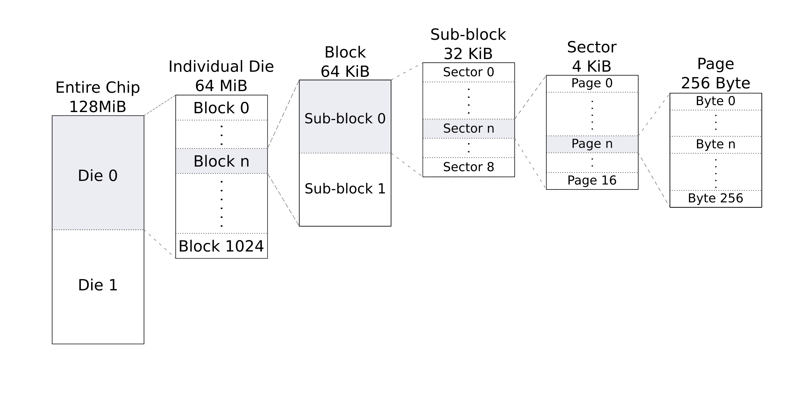
Page, Block and Sector Size (and some definitions)
QSPI NOR memory is organized in various subdivisions or groups of bytes which delineate the minimum and maximum size as well as the address alignment of erase and program operations. In this section, we go over the, not so standard, nomenclature for these regions of memory as well as their typical sizes.
Before going into each subdivision in detail let’s take a look at how a typical large 128 MiB QSPI NOR Flash might be divided. Since this is a large flash, the whole device capacity spans two separate dies of 64 MiB each, think of it as two 64 MiB chips in one. Each die is then divided in 64 KiB blocks and those blocks are further subdivided into two halves of 32 KiB each. This is further subdivided into 4 KiB sectors and those sectors are divided yet again in 256 byte pages. Within those pages we finally find the individual bytes of memory to store our precious data. This is shown in the figure below.
Erase Unit Size
QSPI NOR flash is usually writable down to the individual bytes (except for some ECC protected devices as we’ll see later on). However, like all flash memories, NOR must be erased in large “chunks”. Those chunks can often be subdivided and erased in smaller subunits albeit with a performance penalty. Now, with that being said, manufacturers do not all agree on the naming of those “chunks”. For example, most manufacturers call the largest erasable unit a block, which is usually 64 KiB but can be as big as 512 KiB or even 1024 KiB for ganged multi-die devices. Those same manufacturers also call the smallest erasable unit a sector, which is more often than not 4 KiB. With that caveat in mind, let’s go over the various erase units in more details.
Block
The base erasable unit is usually called a block. The block is the largest group of bytes that can be erased (or flashed) in one operation by the device. The most common block size is 64 KiB but can be as large as 256 KiB. When erasing a larger area than a block with a single QSPI command, QSPI NOR devices internally iterate over each block when erasing.
All modern devices are able to erase smaller sub-unit of the block although with some performance penalty. In other words, erasing a device block by block yields the highest “erase bandwith”. This can be especially important when the NOR flash is hosting a file system as the erase performance has a significant impact on the attainable write bandwidth of a file system. For an in-depth discussion of the subject of this particular topic see the concept section of the TREEspan File System User Manual available in the documentation page.
Sub-Block or Half-Block
Nearly all devices with 64 KiB blocks can erase half a block, or 32 KiB with one command. To make matters confusing, the name of the 32 KiB sub-block appears to be randomly chosen by whomever is writing the datasheet. The 32 KiB sub-block is sometimes called a half-block, a subsector, or even just a block.
Sector
The smallest erasable unit is commonly called a sector. It is, most often than not, 4 KiB, but can be larger for high capacity QSPI NOR and smaller for low-capacity devices. The sector size can be very important when considering a file system for a QSPI NOR flash, as the sector size will define the copy-on-write granularity. Some flash file system or flash translation layer may have upper or lower limits on the supported sector size.
Chip, Device and Die
All single-die QSPI NOR have a command to erase the entire chip, which can be a very long operation, upward of 10 minutes for large devices. The command is usually called chip or device erase and results in each block of the device being erased one after the other. Multi-die devices have a die erase command to erase, as its name implies, a single die. Many multi-die devices, however, do not have a way to perform a full chip or device erase, requiring the software to emit a die erase command for each die in order to erase the entire chip.
Exceptions
There are a few exceptions to the nomenclature described in the preceding paragraphs. Chiefly, Micron calls the largest erasable unit a sector while every erasable subdivisions of a sector are called sub-sectors. This can be confusing as a sector usually refers to the smallest erasable unit by other manufacturers. Cypress also mostly uses the common block/sector nomenclature, except for some very large devices where they inconsistently interchange the term block and sector. Meanwhile, Adesto Technologies call every erasable unit a block regardless of the subdivision. As an additional exception, Adesto also has a few unique devices in their portfolio which are page erasable (256 bytes).
Non-uniform Block Size
Some devices can have a few blocks which are of a smaller size, usually located at the start or at the end of the device. This feature is often optional. In some cases it is selected at manufacturing time, where the non-uniform block size is an option available through a different part number. In other cases, the option is configurable through a register, and often a fuse, to make the configuration permanent. This feature is designed to help support a set of smaller configuration blocks. Those can be used by the application either at boot time or at runtime to store configuration or a boot block.
When using a file system, it is important to be aware of the possible existence of those non-uniform blocks. On some devices, those non-uniform block sizes create a disjoint memory map where smaller blocks must be erased using a different command than normal blocks. On other devices the same erase command can be used for all blocks, but erase speed is much lower for smaller block. The latter case can cause unexpected latency spikes when using a file system.
Write Unit Size
Unlike NAND, NOR Flash can usually be written with a byte granularity. When writing, QSPI NOR devices temporarily store the data to be written in an internal page buffer. This page buffer is then written starting at the address passed along with the page program command. The existence of this page buffer means that NOR cannot write more than a full page buffer worth of data with one command.
Page Size and Write Buffer Length
As mentioned in the previous paragraph, QSPI NOR flash have a maximum number of bytes that can be programmed in one program operation. The same length is used for the page size and is most commonly 256 bytes, although there are devices with 512 byte pages (i.e., Cypress FS-S Eclipse). It’s important to note that while most QSPI NOR support byte address granularity when writing it is not possible for a write operation to cross a page boundary. Overall the page size doesn’t usually have much impact at the software level. A larger page size can help reduce the CPU overhead since fewer commands are required to program the device, however the gains are usually negligible.
ECC Protected Devices.
An important exception to the byte programming granularity of QSPI NOR devices are ECC protected devices which may require writing in aligned chunks of 8 or 16 bytes for the ECC to be calculated and stored correctly. For some devices, such as the Cypress NOR, this is optional as the chip accepts smaller write sizes. In this case, however, ECC protection is disabled on the affected words. For other devices, such as the ECC-enabled W25 from Winbond, it is required to write in aligned multiple of the ECC granularity when ECC is enabled.
Summary Table
To sum everything up, here’s the list of common terms and their usual description, as well as important exceptions.
| Common Name | Description | Exceptions |
|---|---|---|
| Device or Chip | Entire device, including all the dies for multi-die devices. | – |
| Die | Individual silicon die for multi-die devices. | – |
| Block | Largest natural erase unit. | Sometimes called a sector. |
| Sub-block | Largest subdivision of a block, usually half. | Sometimes called a half-block, a subsector or a 32 KiB block. |
| Sector | Smallest erasable unit. | Called a subsector when the manufacturer uses the term sector to refer to the block (See above). Very rarely some devices can erase individual pages. |
| Page | Size of the page buffer and largest amount of data that can be written in one write command. | Very rarely some devices can erase individual pages. |
Confusion with NAND Flash
Because it is such a complex topic, a whole series of articles will be required in the future to cover NAND flash. However, it is important to note a few differences and commonalities between the NAND and NOR naming convention which may be cause for confusion. Thanks to Open NAND Flash Interface (ONFI), the terminology within the NAND world is much more homogeneous. On a NAND chip, there is usually only one erase unit, called simply a block. The same thing is true for the write unit which is always called a page. Contrary to NOR flash, NAND flash cannot be programmed byte per byte and requires an entire page to be written at once. Some NAND do support partial page programming but this is not a physical subdivision of the page.
Also, multi-die devices exist in the NAND world as well. In fact, they are much more common, especially for high density removable storage or SSD. NAND, however, has an additional division called plane which enables improved performance by allowing the same operation to be performed in parallel on two different planes.
Confusion Related to File Systems
Finally, this article would not be complete without mentioning that file systems also have their own convention when naming various chunks of memory. Within the file system world, the word sector is usually used to refer the underlying storage subsystem write and erase block size. The name comes from the era of magnetic storage (floppy disks and hard drives) where a physical sector was a full unit of data along with its ECC or CRC. Very similar to a NAND page nowadays.
On top of that most file systems aggregate sectors into larger units to reduce the space and computing overhead of handling individual sectors. For example the well-known FAT File System uses the term cluster to designate a group of sectors that can be allocated to a file. Modern file systems are not usually as attached to the underlying sector size and may use different terms such as and extent or simply a block when talking about a contiguous group of bytes. The latter should not be confused with the underlying flash block as the two are not tied and often of different sizes.
Conclusion
We hope that this article has presented a good overview of the, rather complex, memory organization of QSPI NOR Flash. The article also highlighted some important areas where the NOR memory organization may be of critical importance when using a file system on a NOR flash. Especially when high performance is desired.
In the next article, we will go over protocol related features with a discussion of fast read and XIP modes.
Click here to read the next article in this series.
If you have any questions or would like some guidance about selecting the best flash device or file system for your application please do not hesitate to contact us.